14-Day
4-Layer PCBA Our Pledge
Faster & Professional Turnkey PCB Assembly Services
Rigid PCBs Manufacturing advantage
- High-Precision Manufacturing
3/3 mil line spacing • 1-32 layers • ±2 mil alignment • HDI/BGA capable
- Industry-Specific Solutions
AEC-Q100 automotive • 5G/RF materials • High-power thermal management
- Quality & Reliability
ISO 9001/IATF 16949 • Full testing (AOI, impedance) • 99%+ yield rate
- Fast Turnkey Service
24h prototypes • 2-7 day production • Stable supply chain
Get DFM analysis and volume discounts
Why Choose Rigid PCBs?
- Robust Structure
Resistant to deformation and vibration, ideal for harsh environments like industrial/automotive applications
- Excellent Electrical Performance
Stable signal transmission, superior high-frequency characteristics, reliable insulation
- High Integration
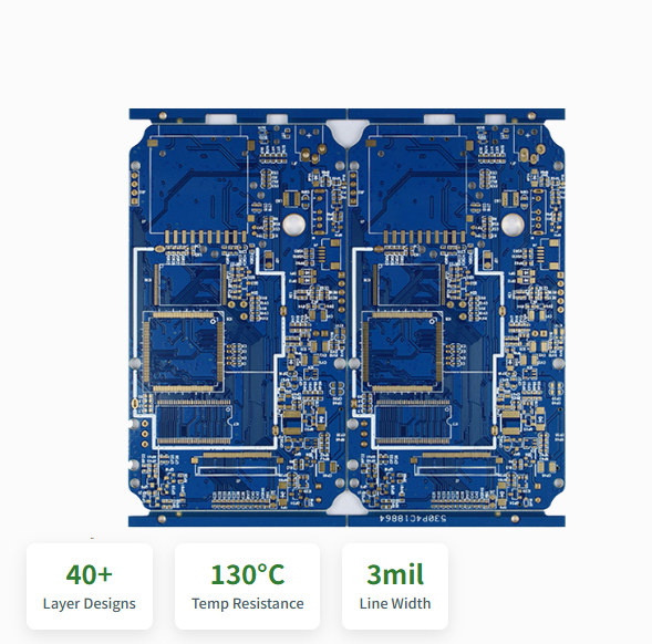
Supports multilayer designs (up to 40 layers) and fine circuitry (minimum 3mil line width)
- Effective Thermal Management
High temperature resistance (130°C+), optional metal substrates for enhanced heat dissipation
Get DFM analysis and volume discounts
Common Materials for Rigid PCBs
Standard Substrates
FR-4 (Fiberglass Epoxy)
- Features: Cost-effective, high mechanical strength, flame retardant (UL94 V-0)
- Applications: Consumer electronics, industrial controls
FR-1/FR-2 (Paper Phenolic)
- Features: Ultra-low cost but poor heat resistance
- Applications: Low-end appliances, simple circuits
High-Frequency Materials
Rogers Series (RO4000, RO3000)
- Features: Low dielectric loss (Df <0.004), stable Dk
- Applications: 5G antennas, satellite communications
Taconic TLY/TLF Series
- Features: Ultra-low loss (Df as low as 0.001)
- Applications: High-frequency filters, aerospace
Our engineers will help select the optimal material
Rigid PCB Manufacturing Process
Precision engineering with 11 critical quality-controlled stages
Material Preparation
- Select substrate (FR-4, Rogers, etc.)
- Copper foil selection
- Cut to required panel sizes
Inner Layer Processing
- Dry Film Lamination
- Exposure & Development
- Acid/alkaline etching
- AOI Inspection
Lamination
- Stack inner layers with prepreg
- Add outer copper layers
- High-pressure (300-500 PSI)
- 180-200°C curing
Drilling
- Mechanical drilling (0.15-6.5mm)
- Laser drilling for microvias (<100μm)
- Deburring and cleaning
Plating
- Electroless Copper Deposition
- Electroplating (20-25μm)
- Through-hole conductivity
Outer Layer Processing
- Repeat dry film process
- Pattern plating
- Final etching
Solder Mask Application
- Screen printing or photoimaging
- UV exposure and development
- Curing (150°C for 30-60 mins)
Surface Finishing
- HASL (Hot Air Solder Leveling)
- ENIG (Electroless Ni/Au)
- OSP/Immersion options
Silkscreen & Marking
- Component labels
- Logos and identifiers
- UV/thermal curing
Testing & Inspection
- Electrical Testing
- 100% visual inspection
- Final QC verification
Packaging & Shipping
- Vacuum sealing
- Desiccant inclusion
- ESD protection