14-Day
4-Layer PCBA Our Pledge
Faster & Professional Turnkey PCB Assembly Services
High-frequency PCB manufacturing services
- Efficiency with Thermally Stable High Frequency PCB
- Professional Surface-mounting and Through-hole soldering
- Various sizes like 1206, 0805, 0603 components SMT
- ICT (In Circuit Test), FCT (Functional Circuit Test)
- PCB Assembly With UL, CE, FCC, Rohs Approval
- Nitrogen gas reflow soldering technology for SMT
- High Standard SMT & Solder Assembly Line
Why Use High Frequency PCB?
- Low Loss: PTFE materials minimize signal attenuation
- High Stability: Heat-resistant with low thermal expansion
- Precise Control: Strict impedance for signal integrity
- Low Dk & Df: Ideal for high-frequency signals
- Anti-Interference: Optimized stacking reduces noise
High-Frequency PCB Material Selection
Optimized for performance based on dielectric properties, thermal stability, and mechanical characteristics
PTFE-Based Materials
Dk:2.0-3.5
Df:0.001-0.005
Applications:Millimeter-wave, Radar
Ultra-low loss
High temp resistant
Modified Epoxy
Dk:3.0-4.0
Df:0.003-0.008
Applications:5G Sub-6GHz, Wi-Fi 6
Cost-effective
Easy processing
Ceramic-Based
Dk:6-10
Df:0.002-0.01
Applications:High-power RF
Excellent thermal
High Dk
Liquid Crystal Polymer
Dk:2.9-3.1
Df:0.002-0.004
Applications:mmWave antennas
Flexible
Low moisture
Polyimide
Dk:3.2-3.6
Df:0.01-0.02
Applications:Flexible circuits
High temp
Durable
High-Freq FR4
Dk:3.8-4.0
Df:0.008-0.015
Applications:Cost-sensitive RF
Low cost
Easy to process
Material Properties Comparison
| Material | Dielectric Constant (Dk) | Dissipation Factor (Df) | Key Applications | Advantages |
|---|---|---|---|---|
| PTFE-Based | 2.0-3.5 | 0.001-0.005 | Radar, mmWave | Ultra-low loss, stable |
| Modified Epoxy | 3.0-4.0 | 0.003-0.008 | 5G, Wi-Fi 6 | Balanced performance |
| Ceramic-Based | 6-10 | 0.002-0.01 | Power amplifiers | High thermal conductivity |
| LCP | 2.9-3.1 | 0.002-0.004 | mmWave antennas | Flexible, moisture-resistant |
| Polyimide | 3.2-3.6 | 0.01-0.02 | Flex circuits | High temp resistant |
| High-Freq FR4 | 3.8-4.0 | 0.008-0.015 | Cost-sensitive RF | Low cost, easy processing |
If you are looking for professional design and manufacturing of Metal Core PCBs
Material Preparation
- PTFE/Rogers materials
- Controlled storage
- Low-profile copper
Dk: 2.0-3.5Df: 0.001-0.005
Inner Layer Processing
- Dry film lamination
- UV exposure
- Plasma etching
±0.05mmAOI inspection
Multilayer Lamination
- Prepreg stacking
- Vacuum press
- 300-400 PSI
180-200°CRO4450B
Precision Drilling
- Mechanical drilling
- Laser microvias
- Desmear process
±25μmCO₂/UV laser
Electroplating
- Electroless copper
- Electroplating
- Via filling
25μm thicknessConductive paste
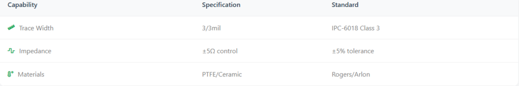
Outer Layer Patterning
- Dry film application
- Fine-line etching
- Impedance control
±5Ω tolerance3/3mil lines
Surface Finish
- ENIG (Gold)
- Immersion Silver
- OSP
0.05-0.1μm AuLow oxidation
Solder Mask
- LPI application
- UV curing
- Registration ±50μm
Green/Black/Blue38-42μm thick
Electrical Testing
- TDR impedance test
- Flying probe test
- Continuity check
±5% tolerance100% tested
Final Inspection
- Microsection analysis
- Moisture barrier bag
- IPC Class 3 standard
100% AOIUL certified
Complete 10-Step High-Frequency PCB Manufacturing Process
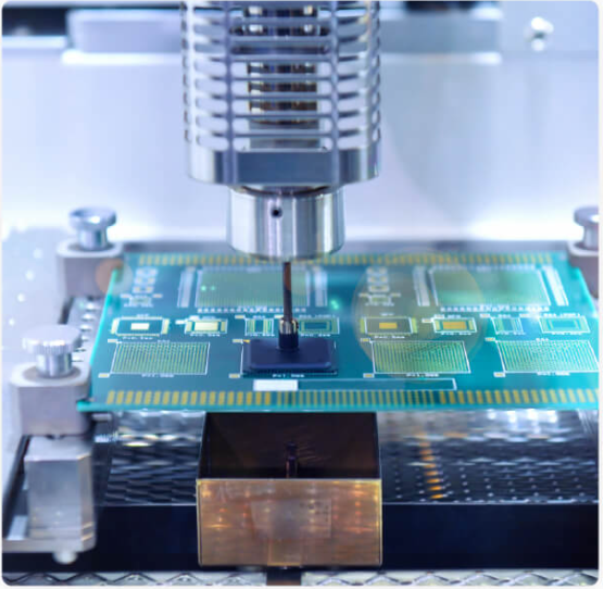
High-Frequency PCB Assembly
End-to-end solutions for RF/microwave applications
1
Material Expertise
- PTFE/Rogers/Ceramic
- Low-Dk laminates
- 2.0-3.5 Dk range
2
Precision Assembly
- 01005 components
- ±0.025mm placement
- RF connectors
3
Quality Assurance
- TDR impedance test
- 3D X-ray inspection
- Military standards