Most engineering teams meet flexible circuits the same way. A product has to fold, a cable harness keeps failing in the field, or the enclosure shrinks until a rigid board no longer fits. The design gets redrawn on thin film, sent out for quote, and comes back with questions nobody asked on the rigid version: copper type, coverlay style, stiffener thickness, bend direction. That is where schedules slip. The inputs a flexible PCB supplier needs are mechanical as much as electrical.
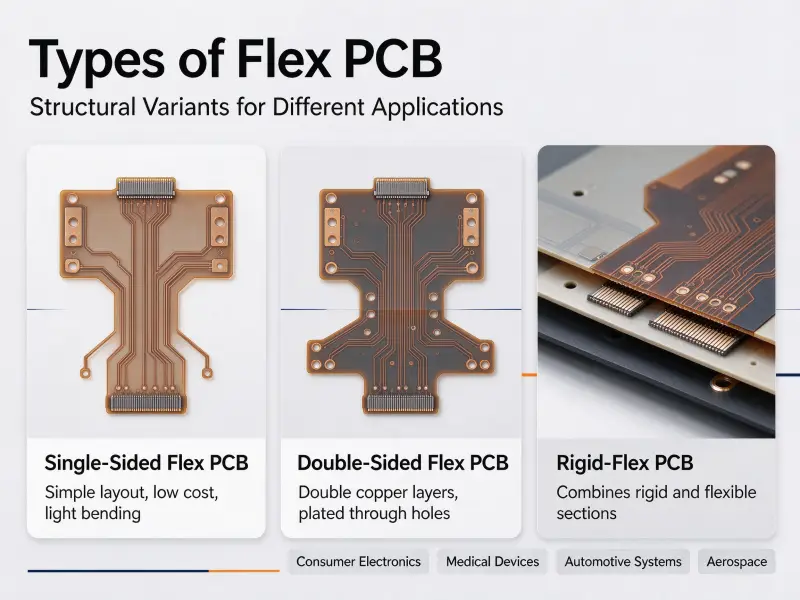
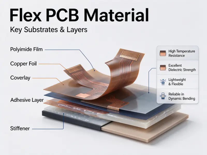
Flexible PCB manufacturing is the production of a circuit on a thin polymer film rather than a rigid glass-epoxy core. Copper is bonded to polyimide or polyester, imaged and etched into traces, laminated under a protective cover film, and reinforced with stiffeners only where components or connectors need support. The finished board bends, folds, and survives motion that would crack a rigid board.
This guide follows the work from material selection through fabrication, design limits, termination, and price.
What flexible PCB manufacturing produces
The output is a single-sided, double-sided, or multilayer circuit on flexible substrate, usually between 0.1 mm and 0.3 mm thick, that carries current, routes signals, and replaces the cables and connectors a rigid design would need.
Production runs on panels like any other board, so the equipment looks familiar. What changes is handling. There is no glass cloth to hold dimensions, the material arrives on rolls and moves under tension, and every lamination cycle can trap air, shift registration, or cure adhesive unevenly. The market shows how much of modern PCB electronics now depends on it: the flexible printed circuit board market reached $31.07 billion in 2026, up from $28.36 billion in 2025 (The Business Research Company, 2026).
How the layers stack up
| Layer | Function | Typical specification |
|---|---|---|
| Base film | Carrier and dielectric | Polyimide 12.5–50 µm; polyester for static parts |
| Copper foil | Conductors | 12–35 µm, rolled annealed where the part moves |
| Adhesive | Bonds copper to film | 20–25 µm, omitted in adhesiveless laminates |
| Coverlay | Protects traces, opens pads | 25 µm polyimide film, or photoimageable covercoat |
| Stiffener | Rigidity at connectors and SMT | FR4, polyimide, or steel, 0.1–0.25 mm |
| PSA | Bonds flex to housing | 25–50 µm pressure-sensitive adhesive |
Where flexible circuits get used
| Application | Mechanical demand | What it does to the design |
|---|---|---|
| Wearables and hearables | Tight folds, repeated motion | Single layer, thin film, rolled annealed copper |
| Automotive sensors | Vibration and thermal cycling | Stiffened tails, wider traces, higher class |
| Catheters and instruments | Miniaturisation, sterilisation | Adhesiveless laminate, fine lines |
| Print heads and cameras | Continuous reciprocating motion | Long dynamic zone, no vias in the bend |
Flexible PCB materials and what each layer does
Material choice sets flex life, temperature range, and price before a single process step runs, so it belongs in the design review rather than the purchasing conversation.
Polyimide is the default for anything that survives soldering or moves repeatedly. Polyester is cheaper and adequate for parts that bend once during assembly and then stay put.
| Property | Polyimide | Polyester |
|---|---|---|
| Service temperature | Around 260 °C, survives reflow | Around 150 °C, reflow not suitable |
| Dynamic flex life | High | Limited, static bends only |
| Moisture uptake | Low | Higher |
| Typical use | Automotive, medical, multilayer | Low-cost static interconnects |
Copper matters as much as film. Rolled annealed foil has an elongated grain that resists fatigue, while electrodeposited foil has a columnar grain that is cheaper and fine for static bends but cracks under repeated strain. Any copper in a zone that moves gets rolled annealed foil.
The cover layer decides how well traces are protected. A polyimide coverlay bonded with adhesive gives the longest flex life and the most forgiving process, at the cost of wider opening tolerances. A photoimageable covercoat resolves finer features and sits thinner, which suits dense static designs but shortens life in a bend. Finishes follow the same logic: ENIG for general pads, OSP where flatness matters more than shelf life, hard gold on contact fingers only.
Stiffeners solve a mechanical problem. FR4 adds a rigid pad behind components and connector tails, polyimide gives support with a thinner profile, and stainless steel spreads heat in LED sections. PSA bonds the finished part into a housing and cannot be reworked once applied.
The flex PCB fabrication process, step by step
Fabrication follows the rigid board sequence up to imaging, then diverges at coverlay lamination, where a flexible protective film replaces solder mask and the panel has to stay flat while it cures.
- Material cutting. Film is cut from roll to panel and baked to remove moisture before lamination.
- Drilling. Mechanical drills reach 0.1 mm; lasers form microvias in thin dielectrics. Backing materials protect the soft film from burrs.
- Imaging and etching. Dry film resist is exposed and developed, then copper is etched to leave traces. Artwork is compensated for etch factor and film shrinkage.
- Plating. Copper is plated through holes and over traces, followed by the selected finish.
- Coverlay lamination. A pre-patterned coverlay is registered to the pads and pressed under vacuum, then cured. Registration here is the most common source of scrap.
- Surface finish. ENIG, OSP, or hard gold is applied to exposed pads and contacts.
- Stiffener and PSA attachment. Pre-cut stiffeners are bonded and cured; PSA goes on where the part will be mounted.
- Profiling. Laser, punch, or rout separates parts. Edges must be clean, because a burr becomes a crack origin.
- Test and inspection. Open and short testing, impedance checks where specified, microsection, and visual inspection.
Where flex processing diverges from rigid
Most PCB learning material describes rigid lamination, and flex departs from it in three places. Polyimide moves more than FR4, so artwork is scaled to compensate for shrinkage rather than corrected afterwards. Without glass cloth the film has no dimensional anchor, which puts a premium on low-tension transport and fixtures that support the panel instead of stretching it. Coverlay registration tolerances are wider than solder mask tolerances, and that has to be reflected in pad design rather than argued about at first article. The failure signatures point the same way: delamination from cure pressure, copper cracking from handling damage, adhesive squeeze-out from press pressure, voids under stiffeners from trapped air.
Flexible PCB thickness and how to specify it
Total thickness is the sum of base film, copper, adhesive, coverlay, and any stiffener, and it sets the minimum bend radius, the impedance, and the fit inside the enclosure.
A single-sided build with 25 µm film, 18 µm copper, and a 25 µm coverlay with 25 µm adhesive lands near 0.09 mm. Add a second copper layer and a bonding adhesive and the same construction moves to roughly 0.15 mm. Most flexible PCB boards sit between 0.1 mm and 0.3 mm; thin single-sided parts go below 0.1 mm, while multilayer or heavily stiffened builds run past 0.5 mm.
Thickness tolerance and what belongs on the drawing
Thickness stacks, so the tolerance stacks. State a total for each zone, because the bend area, the stiffened connector area, and any pad area will not measure the same. Give the measurement points, say whether the stiffener is included, and put the target on the finished part rather than the laminate. A drawing that says 0.2 mm with no datum and no zone map produces a first article argument instead of a board.
Design rules that decide whether the flex survives
Bend radius predicts life and is calculated from total flex thickness: a common starting point is six times the thickness for a one-time static bend and one hundred times for a part that flexes continuously.
| Construction | Static bend | Dynamic flex |
|---|---|---|
| Single layer | 6× total thickness | 100× total thickness |
| Two layers | 10× to 12× | 100× to 150× |
| Three or more | 20× to 25× | Not recommended without review |
The multipliers follow IPC-2223 guidance as it is usually cited; suppliers interpret the edges differently, so the drawing should state the radius you need and let the fabricator confirm it. Radius is measured from the inside of the bend, and a 20% to 30% margin absorbs material and assembly variation. A 0.15 mm single-layer part with a static bend needs about a 0.9 mm radius at the guidance, or 1.1 mm to sit comfortably.
Routing through the bend zone
PCB board design for a moving part starts at the bend, not the schematic. Traces cross the bend line at 90 degrees, because angled routing concentrates strain along one edge of the conductor. Sharp corners become arcs or chamfers. Traces on opposite layers are staggered so they do not form a stiff beam, vias stay out of the bend, and solid ground planes become hatched planes so copper still provides a reference without locking the film. Teardrops at pad-to-trace junctions cost nothing and prevent cracking at a sharp transition. Components belong on stiffened areas, and the rigid-to-flex line is a keep-out for pads and vias.
What dynamic bending does to cycle life
Static and dynamic are not neighbouring cases. A part bent once at installation accumulates a single strain; a part that flexes in service accumulates it thousands of times, and copper fatigue follows a power law, so a small reduction in strain buys a large increase in cycles. That is why dynamic flexible PCB design stays at one or two layers, keeps plated holes out of the moving zone, and accepts a much larger radius.
Flexible PCB connectors and termination options
Termination is the part of flexible PCB design most often under-specified, and it decides whether the assembly survives mating, vibration, and rework.
| Termination | Where it fits | What to specify |
|---|---|---|
| ZIF connector | Board-to-board, serviceable assemblies | Finger thickness, stiffener, gold, insertion depth |
| Direct tail solder | Permanent, few mating cycles | Pad anchoring, strain relief, wicking control |
| Hot bar bonding | High pad count, thin profile | Pad flatness, bond window, rework plan |
| Press-fit or spring contact | Vibration, field service | Stiffener, wear-resistant plating, coplanarity |
Every flexible PCB circuit ends somewhere, and the connector datasheet covers the housing rather than the board. The flex drawing has to carry the stiffener thickness under the contacts, the gold thickness on the fingers, the chamfer that guides insertion, the mating cycles expected, and coplanarity across the contact row. Those five items decide whether the part mates on the line or in the rework station.
What drives flexible PCB price
There is no standard flexible PCB price. The quote is a function of layer count, panel utilisation, material grade, termination complexity, and test scope, and two boards with the same layer count can sit far apart.
| Cost driver | Why it moves the price | How to control it |
|---|---|---|
| Layer count | Each layer adds lamination and drilling | Keep the flex zone at one or two layers |
| Panel utilisation | Odd shapes waste film | Nest parts and share arrays |
| Material grade | Adhesiveless polyimide and RA copper cost more | Use polyester where the part is static |
| Coverlay type | Patterned coverlay needs tooling | Covercoat where flex life is not limiting |
| Termination | Stiffeners, gold, and bonding add steps | Standardise stiffener thickness |
| Test scope | Impedance and bend cycling add time | Match the plan to the acceptance class |
How to compare flex quotes fairly
A price is only comparable when the inputs match. Send the same pack to every supplier: stackup drawing with bend zones marked static or dynamic, layer count, film and copper type, coverlay type, stiffener specification, finish, thickness by zone, acceptance class, test plan, annual volume, and array preference. Without the zone map, one quote may assume a static part and another a dynamic one, and the gap will look like pricing when it is specification.
Flex, rigid, or rigid-flex
Flex suits a board that has to move or fit a shape; rigid-flex suits a fold that has to replace a connector between two rigid sections.
| Rigid | Flex | Rigid-flex | |
|---|---|---|---|
| Substrate | FR4 | Polyimide film | FR4 plus polyimide |
| Typical thickness | 0.8–3.2 mm | 0.1–0.3 mm | 0.5–2.4 mm |
| Bending | None | Throughout | Flex zones only |
| Interconnect | Headers and cables | ZIF or soldered tail | Continuous, no connector |
The economics turn on connectors. A pure flex replaces a cable and two connectors with one part. A rigid-flex goes further and removes the connector between two boards, but a rigid-flex PCB manufacturer has to laminate dissimilar materials in one cycle, which adds tooling and yield risk. That trade only pays when the connector it removes is a real failure point or a real assembly cost.
How to qualify a flexible PCB manufacturer
Qualification is a set of specific questions about process limits and test evidence, not a certification logo on a homepage.
Start with the acceptance class the supplier builds to by default. IPC-6013, the qualification and performance specification for flexible and rigid-flexible printed boards, classifies construction by type, performance by class, and installation by use. The class drives copper width tolerance, annular ring, and coverlay adhesion, and the usage category is what justifies rolled annealed copper over electrodeposited. A drawing that names only the class leaves the material decision to the fabricator.
Then ask for what the line actually holds: layer count, minimum trace and space, minimum laser drill, coverlay registration tolerance. Ask whether microsection, impedance, and bend-cycle data ship with the order, which laminate family is standard, and whether adhesiveless material carries a lead-time penalty. Confirm ISO 9001, and add IATF 16949 or ISO 13485 where the product demands it. Finally, ask how first article and engineering changes are handled, because a flexible PCB board usually changes once after the first mechanical fit.
Frequently asked questions
Is an FPC the same thing as a flexible PCB?
Yes. FPC stands for flexible printed circuit and describes the same object as flex PCB or flexible circuit. The abbreviation is more common in Asian supply chains and on drawings that specify a bare flex without stiffeners or assembly, while flexible PCB appears in procurement documents. The construction does not change with the name.
Can a flexible PCB carry components on both sides?
It can, with conditions. Double-sided placement needs stiffeners behind both component areas, pad anchoring that survives reflow, and low-mass parts. Once a design needs dense placement on both sides, a rigid-flex section is often cheaper than a fully stiffened flex, because the rigid area carries the components and only the interconnect stays flexible.
What is the minimum order quantity for a custom flex design?
There is no industry standard. The floor is set by panel utilisation and tooling: coverlay patterns, stiffener dies, test fixtures, and setup time on each lamination cycle. Simple single-sided parts run in prototype quantities, while multilayer builds become economical once tooling spreads across a larger order. The useful question is the quantity at which the per-piece price stops falling.