A flexible PCB is a thin circuit built on plastic film instead of glass-reinforced epoxy, and it exists because most enclosures have no flat, rigid place for electronics. Buyers usually arrive at the type question with a drawing and a bend line already sketched, then get handed a list of build names that reads like a difficulty ladder. Picking the most capable option to be safe is the usual mistake.
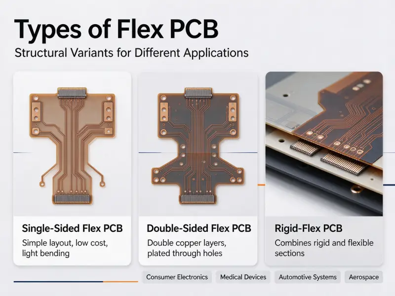
There are five standard types of flex PCB, separated by IPC-6013 as Type 1 through Type 5: single-sided, double-sided, multi-layer, rigid-flex, and HDI flex. The correct type is not the most advanced one. It is the one that matches how the circuit moves, how many copper layers the routing needs, and whether the assembly also needs a stiffened area to hold components.
Before comparing the five, it helps to see what a flexible PCB supplier actually starts with, because every type is a variation on one stack of film and copper.
What makes a flex PCB different from a rigid board
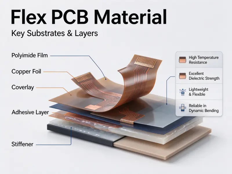
A rigid board uses woven glass and epoxy to hold its shape. A flex PCB bonds copper to a thin polymer film, so the circuit can bend without cracking. Everything else follows: the copper has to be ductile, the protective layer has to be a laminated film, and any section that must stay flat has to be stiffened.
A 1.6 mm FR-4 board survives assembly because it does not move. A flexible pcb board at 0.1 mm needs carriers at every process step and warps if the copper is unbalanced.
| Attribute | Rigid PCB (FR-4) | Flexible PCB (polyimide) |
|---|---|---|
| Base material | Glass and epoxy, 0.2 to 2.0 mm | Polyimide film, 12.5 to 50 µm |
| Copper | Electro-deposited, 1 oz typical | Rolled annealed, 0.5 oz typical |
| Protective layer | Printed solder mask | Polyimide coverlay |
| Thickness | 0.4 to 2.4 mm | 0.05 to 0.5 mm |
| Heat tolerance | Tg of 130 to 180°C | About 260°C continuous |
The layers that decide everything
Four decisions in the flexible pcb material stack drive most of the cost and nearly all of the bend life.
- Copper type. Rolled annealed copper survives repeated flexing. Electro-deposited copper is cheaper but cracks earlier.
- Adhesive or adhesiveless. Acrylic laminates cost less. Adhesiveless stacks hold finer lines and take higher reflow temperatures.
- Cover layer. A coverlay protects traces but adds thickness in the bend zone. A photoimageable mask is thinner.
- Stiffeners. FR4, polyimide, stainless or aluminum under connectors, for insertion force.
Flexible pcb thickness sets the bend radius, so a stiffener in the wrong place can halve the radius you have left.
The five flex PCB types at a glance
IPC-6013 groups flexible boards into Types 1 through 5. Type 1 is single-sided, Type 2 is double-sided, Type 3 is multi-layer, Type 4 is rigid-flex, and Type 5 is HDI flex with build-up layers. A design falls into a group on copper layer count and on whether the board carries rigid sections, not on order size.
The IPC 6013F specification covers all four laminated constructions, including stiffeners, plated through-holes, microvias and blind or buried vias. It does not tell you which one your product needs.
| Type | Copper layers | Bend duty | Relative cost | Typical use |
|---|---|---|---|---|
| Type 1, single-sided | 1 | Static and dynamic | Lowest | Ribbon links, print heads, LED strips |
| Type 2, double-sided | 2 | Mostly static | Low to mid | Camera modules, clusters, wearables |
| Type 3, multi-layer | 3 to 8 | Static, bend-to-fit | Mid to high | Impedance-controlled RF, medical imaging |
| Type 4, rigid-flex | Rigid plus flex | Install bend, limited dynamic | Highest | Aerospace, foldables, robotics |
| Type 5, HDI flex | 1 to 2 plus build-up | Static | High | Miniaturised sensor modules |
The cost column is relative within flex. Every entry costs more than a rigid board of the same outline.
Single-sided flex PCB (IPC Type 1)
A single-sided flex PCB has one copper layer bonded between two polyimide films, with no plated through-holes. It is the cheapest flex construction, and in dynamic bending it is also the most durable, because the only copper layer sits near the neutral axis where bending stress is close to zero.
This is the type that gets overlooked. Engineers assume one layer cannot be serious, jump to double-sided, and lose bend life for routing freedom they did not need. Access openings can sit on one face, both faces, or as unsupported fingers for a connector.
Where it stops working
- No cross-layer routing, so there is no real ground plane and return paths get long.
- Components mount on one face, and anything heavier than a small passive needs a stiffener.
- Exposed connector fingers fatigue under repeated insertion.
Double-sided flex PCB (IPC Type 2)
A double-sided flex PCB puts copper on both faces of the film and connects the layers with plated through-holes. It roughly doubles the routing available in the same outline, which makes it the most common flex build, but those holes become crack initiation points wherever the board bends.
The stack is coverlay, copper, core, copper, coverlay. The sweet spot is a board that folds once during installation and then stays put.
Routing density against bend life
Polyimide’s dimensional instability makes layer-to-layer registration harder than on FR-4. Keep every plated hole out of the bend zone, and if the board has to cycle, confirm the flexible pcb design against bend test data.
Multi-layer flex PCB (IPC Type 3)
A multi-layer flex PCB stacks three or more copper layers with flexible dielectric between them. It is the only flex construction that supports controlled impedance with dedicated ground and power planes, and it also loses bend capability fastest as layers are added.
Blind and buried vias, stripline routing and tighter impedance tolerances all become available here, which is why the type turns up in RF front ends, medical imaging heads and harness replacements. A four-layer stack that routes beautifully may be unusable in a 2 mm radius.
HDI flex, Type 5 in practice
HDI flex adds laser-drilled microvias, thinner dielectrics and lines down to a few mils. It is what makes camera actuators and implantable sensor modules possible, and it is the wrong answer for anything that flexes in service.
Rigid-flex: when one board replaces three
A rigid-flex board laminates rigid FR-4 sections onto flexible polyimide layers as one continuous stack. Components and connectors mount on the rigid areas, the flex areas act as the hinge, and the board-to-board connectors that used to join separate boards disappear.
Coverlay is applied only over the flexing regions, and plated through-holes can run through both rigid and flexible layers. A rigid-flex PCB manufacturer builds this as a single laminated part, which is the point: fewer parts, fewer joints, fewer things that fail in vibration.
| Consideration | Flex plus connector | Rigid-flex |
|---|---|---|
| Parts in the assembly | Boards plus connector and cable | One laminated board |
| Assembly steps | Separate SMT runs, then mating | One SMT run |
| Failure points | Contacts, solder joints, cable flex | Trace fatigue at the transition |
| Unit board price | Lower | Higher |

Rigid vs. flex PCB: the difference that decides the quote
A rigid PCB holds its own shape and carries everything on a flat plane. A flex PCB bends to fit the space the enclosure allows. The difference is economic: a rigid design buys cheap boards and then spends on connectors, cables and assembly steps, while a flex design does the reverse.
| Factor | Rigid PCB | Flex PCB |
|---|---|---|
| Base material | FR-4 | Polyimide, sometimes PET |
| Thickness | 0.4 to 2.4 mm | 0.05 to 0.5 mm |
| Interconnects | Connectors and harnesses | Traces run through the bend |
| Repair | Rework is routine | Rework damages pads |
| Board price | Baseline | Three to eight times higher |
| Best fit | Static, cost-driven volume | Moving or curved assemblies |
A flex circuit that removes two connectors and a harness can cost more per square inch and still land cheaper per finished unit.
What are the downsides of using flexible PCBs
The downsides are price, dimensional instability during fabrication, limited repairability, tighter handling requirements, and a bend life that depends on design details rather than on the material. Each has to be designed around rather than inspected out at the end.
- Higher unit cost. Polyimide, RA copper, coverlay, stiffeners and extra process steps cost more than their FR-4 equivalents.
- Dimensional instability. Polyimide expands and shrinks with humidity and heat, so yields run below rigid board rates.
- Poor repairability. Repeated rework lifts pads and delaminates coverlay. Treat the board as single-use.
- Handling and fixturing. Thin film needs carriers, a pre-bake before reflow and slower line speeds.
- Bend life depends on design. Trace direction, via placement and radius move cycle counts by orders of magnitude.
Are flex PCBs more expensive?
Yes. A flex PCB costs several times more than a rigid board of comparable size and layer count, and published fabricator pricing guides usually put the gap at three to eight times. The premium comes from materials and process steps, not from margin.
A rigid board starts at roughly $2 per square foot of laminate. A flexible pcb manufacturer quotes against polyimide film instead, at about $6 to $60 per square foot before any processing.
| Cost driver | Effect on flexible pcb price |
|---|---|
| Base material | Polyimide costs several times more per unit area |
| Layer count | Each layer raises material use and lamination risk |
| Coverlay processing | Lamination and laser opening add steps |
| Panel utilisation | Small or irregular outlines waste panel area |
The premium can disappear once pcb manufacturing moves up to assembly level. Connector elimination, harness reduction and lighter weight offset board price, and the offset grows with volume. Price the decision on installed cost per unit, which means quoting both builds from the same drawing.
When to use a flex PCB
Use a flex PCB when the circuit has to move, fit a curved or folding space, lose weight, or replace a connector and cable run. Stay on FR-4 when the board sits still and volume is high, because nothing in a flex build pays back motion the product does not need.
Signals that point to flex:
- Any part of the board moves, hinges or cycles in service.
- The space is curved, stepped or thinner than 0.5 mm.
- Weight matters, as in wearables or handheld instruments.
- Board-to-board connectors have to go to survive vibration.
Signals that point back to rigid:
- The board never moves after installation.
- Component density and thermal load leave no room for stiffeners.
- Rework and field repair are expected.
Fix the motion requirement first, then the layer count the routing demands, then the thickness that fits the envelope.
Thickness and bend radius: the numbers that pick your type
Finished thickness sets the minimum bend radius, and the radius is a multiple of that thickness. The multiple changes with construction and with whether the bend happens once during assembly or a million times in service. Designers who lock thickness before checking the radius usually end up redesigning.
| Construction | Static minimum radius | Dynamic minimum radius |
|---|---|---|
| Single-sided | 6 to 10 times thickness | About 100 times thickness |
| Double-sided | 10 to 12 times thickness | Not recommended for cycling |
| Multi-layer and rigid-flex | 20 times thickness or more | Not recommended |
Those multiples come from IPC-2223 design practice. Final values depend on copper weight and coverlay thickness, so confirm them against the fabricator’s bend test data before tooling.
- Route traces perpendicular to the bend line, never parallel to it.
- Keep plated through-holes and vias out of the bend zone.
- Use hatched ground planes rather than solid copper pours in bending areas.
- Balance copper symmetrically about the neutral axis, and keep stiffeners and coverlay openings out of the bend.
FAQ
Can components be soldered directly onto a flex PCB?
Yes, with conditions. Standard SMT reflow works on a polyimide pcb circuit, but the film absorbs moisture, so panels need a bake before reflow or the coverlay can blister. Components are usually limited to stiffened areas, and the stiffener has to be specified in the PCB board design from the start.
What is a flexible PCB connector, and which one should I specify?
The common choice is a ZIF connector, which clamps the flex tail without sliding contacts across the pads. Pitch runs from 0.3 mm to 1.0 mm, and pin count and available height usually decide.
What files does a fabricator need to quote a custom flex PCB?
Gerber or ODB++ data, a stack-up drawing with copper weight and coverlay thickness, stiffener locations, the bend line and whether the bend is static or dynamic, plus finish, impedance targets and quantity. If you are still in the pcb learning stage, send the mechanical envelope too, so a type mismatch gets flagged early.