Flexible PCB projects rarely fail at the schematic stage. They fail later, when a board that worked flat on a bench starts cracking at the bend line, or when the quote comes back well above the rigid version. Both trace back to what the board is made of. Teams ordering a custom FPC often send a drawing full of dimensions with one line that simply reads “polyimide.”
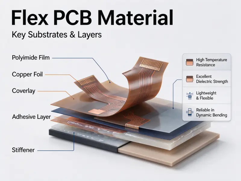
Flex PCB material is a stack of four functional layers, plus two optional ones: a dielectric base film such as polyimide, an adhesive layer or none at all in a two-layer laminate, a copper foil conductor, and a coverlay or solder mask, then stiffeners and a surface finish where the design needs them. Base film and copper decide how the board bends. Adhesive, coverlay and stiffener decide how thick it gets and how well it survives assembly.
The stack is easier to follow from the bottom film up.
What a flex PCB stack-up is made of
A single-sided flexible PCB is base film, copper and coverlay. Every other layer exists to fix a problem those three cannot.
Most stack-up drawings repeat the same six rows, and almost every argument about flexible pcb thickness or bend life traces back to one of them. Plenty of pcb learning material stops at the film and never explains the rest.
| Layer | Typical materials | Thickness | What it controls |
|---|---|---|---|
| Base film | polyimide, PET, PEN, LCP | 12.5-125 µm | bend life, temperature rating, dielectric loss |
| Adhesive (optional) | acrylic, epoxy, modified epoxy | 12-25 µm | bond strength, final thickness, outgassing |
| Copper foil | rolled annealed or electro-deposited, 1/2-2 oz | 17-70 µm | current capacity, flex fatigue |
| Cover layer | polyimide coverlay, photoimageable coverlay, LPI mask | 10-75 µm | trace protection, fine-line resolution |
| Stiffener (optional) | FR-4, polyimide, aluminum, stainless steel | 0.1-1.6 mm | connector and component support |
| Surface finish | ENIG, OSP, immersion tin | 0.05-6 µm | solderability, contact resistance |
Every flexible pcb material choice sits in one of those rows. Flexible pcb manufacturing also prices them differently from FR-4, because film is bought by area and laminated in a press rather than plated up.
Base film: polyimide, PET, PEN and LCP
Polyimide is the default for anything that bends more than once. PET covers cost-driven designs that fold once. PEN sits between them. LCP answers a different question, high-frequency loss, and gives up some flex life to do it.
Film choice sets the ceiling on everything else. A base film rated to 120°C cannot be rescued by a better coverlay.
| Property | Polyimide | PET | PEN | LCP |
|---|---|---|---|---|
| Continuous service temperature | ~260°C | 105-125°C | 150-200°C | 200-280°C |
| Glass transition | 360-410°C | 67-80°C | ~120°C | 220-280°C |
| Dielectric constant, 1 MHz | 3.4-3.5 | 3.0-3.5 | ~3.2 | 2.9-3.1 |
| Moisture absorption | 1.5-3.0% | 0.3-0.8% | 0.2-0.4% | 0.04-0.1% |
| Published flex life | 100,000+ cycles | 1,000-10,000 | limited | 10,000-100,000 |
| Relative film cost | 1.0 | 0.3-0.5 | above PET, below PI | 2-3 |
Those numbers come from laminate datasheets and move with grade. Use them to shortlist, then confirm with a bend test.
Polyimide, the default for anything that bends
Polyimide is a thermoset. After curing it stays flexible instead of going brittle, which is why it survives repeated bending and lead-free reflow at roughly 260°C. The weakness is water. It absorbs 1.5-3.0% by weight, and that moisture turns to steam during reflow, so boards left in a humid room without a bake come out blistered.
PET and PEN, the cost tier
Polyester costs a fraction of polyimide but cannot take reflow. At 105-125°C it belongs in boards that fold once and stay put: jumper tails, battery tabs, static connectors. PEN raises the ceiling, keeps most of the cost advantage, and suits static designs that run warmer.
LCP for high frequency
Liquid crystal polymer absorbs almost no water and holds a stable dielectric constant into millimeter-wave frequencies, which is why it appears in antenna modules and radar boards. It also bends less well than polyimide, the lamination window is narrow, and fewer laminators stock it, so the flexible pcb price climbs.
Halogen-free and RoHS constraints
European RoHS rules have restricted six substances, including brominated flame retardants, in electronics sold in the EU since July 2006. Laminate, coverlay, prepreg and stiffener all need a halogen-free grade, not just the base film. Ask for the declaration with the quote, not after the first shipment.
Adhesive or no adhesive: two-layer and three-layer laminates
A three-layer laminate is film, adhesive and copper. A two-layer laminate bonds copper straight to the film, so it is thinner, more stable in heat and more expensive.
The adhesive is the weak link in a three-layer laminate. Acrylic systems soften at temperatures the polyimide shrugs off, add 12-25 µm to the dielectric, and can outgas in vacuum processes.
| Property | Three-layer (with adhesive) | Two-layer (adhesive-free) |
|---|---|---|
| Dielectric build | film plus 12-25 µm adhesive | film only, 12.5-125 µm |
| Heat resistance | limited by the adhesive | higher, more reflow margin |
| Dimensional stability | worse | better |
| Flex performance | good | depends on construction |
| Material cost | lower | higher |
| Availability | broad | narrower, longer lead time |
Adhesive-free usually wins on thickness and fatigue in a dynamic zone. For a static board that folds in assembly, three-layer material is cheaper and does no harm. Flexible pcb design reviews argue about copper while the laminate construction quietly decides half the outcome.
Copper foil: rolled annealed against electro-deposited
Rolled annealed copper bends. Electro-deposited copper etches fine. Choose by whether the trace has to survive motion.
Rolled annealed foil is rolled to thickness, so its grains run long and flat, and a crack has to travel across them. Electro-deposited foil is grown on a drum with a nodular, fish-scale surface: cheaper at fine line widths, but it cracks earlier under cyclic strain.
| Foil | Grain structure | Best use | Typical weight |
|---|---|---|---|
| Rolled annealed | columnar, elongated | dynamic flex, bend zones, cables | 1/2-2 oz |
| Electro-deposited | nodular, low profile | static flex, fine pitch, HDI flex | 1/2-2 oz |
At a fixed bend radius, strain rises with copper thickness, so a 2 oz trace in a moving zone cracks sooner than a 1/2 oz trace. If a pcb circuit needs current capacity in a bend area, parallel traces beat thicker copper.
Coverlay, solder mask and stiffeners
The cover layer is a mechanical part, not just a coating. Stiffeners are what let a flex board hold a connector or carry an SMT part without flexing under it.
| Cover option | Thickness | Resolution | Dynamic flex | Tooling |
|---|---|---|---|---|
| Polyimide coverlay with adhesive | 25-75 µm | around 4 mil lines | yes | opening die or laser program |
| Photoimageable coverlay | 25-50 µm | 2-4 mil lines | good | imaging only |
| LPI solder mask | 10-30 µm | finest | static only | standard |
Coverlay film, photoimageable coverlay and LPI
A laminated polyimide coverlay is the durable option most dynamic designs use. It needs an opening for every exposed pad, cut with a die or a laser, which adds non-recurring cost and lead time. Photoimageable coverlay skips the die. Liquid photoimageable solder mask is the cheapest and finest of the three, but it is a brittle epoxy system for static flex only.
Registration decides yield on fine pitch. A shift of about 0.05 mm can expose the edge of an adjacent trace, and the short often shows up only after the product ships. Keep the coverlay 0.15-0.25 mm past the outermost conductor.
Stiffeners and surface finishes
Stiffeners turn a floppy tail into something a connector can grip. FR-4 is the cheap default, polyimide stays thin and tolerates heat, aluminum spreads heat, and stainless steel gives the most strength at a flexible pcb connector. Thickness commonly runs from 0.1 mm to 1.6 mm.
Surface finish matters less than teams expect. ENIG dominates flex because the nickel barrier is ductile and flat enough for fine pitch. OSP and immersion tin suit cost-sensitive static boards. Hot-air leveling is used less on thin film, since thermal shock works against a fragile stack.
What actually sets flex PCB thickness
Flexible PCB thickness is the sum of the films, adhesives and copper in the stack, plus whatever stiffener is bonded on top. It is not a single number you can order from a catalogue.
Most builds land between 0.05 mm and 0.5 mm. Above that, the thickness usually comes from a stiffener or a multilayer build rather than the flex core.
| Element | Thickness |
|---|---|
| Polyimide base film | 25 µm |
| Rolled annealed copper, 1/2 oz | 17 µm |
| Coverlay film plus adhesive | 25 + 25 µm |
| Plating and finish | 3-5 µm |
| Total | about 0.10 mm |
Bond a 0.8 mm FR-4 stiffener behind the connector and the local thickness becomes roughly 0.9 mm. Drawings therefore dimension the flex zone and the stiffened zone separately, with about ±0.05 mm on each.
Why flex material costs more than rigid
Flex costs more per unit area, and the gap comes from film prices, extra lamination steps and lower yields, not from copper.
Five items drive most of the difference.
- Base film is a specialty product sold by area and costs far more than FR-4 laminate of the same size.
- Two-layer adhesive-free laminate carries a premium over three-layer material.
- Coverlay openings need a die or a laser program, which is non-recurring tooling.
- Thin panels run on carrier plates, so labor rises, and misregistration, wrinkles and creases scrap panels a rigid process would have passed.
- Stiffener bonding, often a second lamination, adds steps.
The savings sit elsewhere: connectors removed, harnesses deleted, brackets gone, assembly time down, weight down. A flexible pcb price should be compared as installed cost, not board price. In pcb electronics the board is a small slice of the build, and the assembly it replaces often costs more than the flex premium. No standard multiplier connects the two prices, so send a full stack-up instead of asking for a rule of thumb.
Rigid, flex and rigid-flex compared
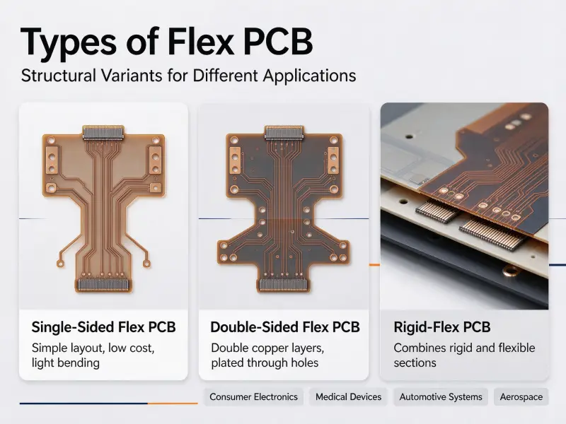
Rigid boards use FR-4 and hold their shape. Flex uses film and folds. Rigid-flex laminates both into one board, so a flex tail carries signals between rigid sections.
| Attribute | Rigid | Flex | Rigid-flex |
|---|---|---|---|
| Substrate | FR-4 or CEM | polyimide, PET, LCP | FR-4 plus polyimide |
| Typical thickness | 0.4-1.6 mm | 0.05-0.5 mm | mixed by zone |
| Bending | none | static or dynamic | flex zone only |
| Protective layer | LPI solder mask | coverlay or LPI | both, by zone |
| Stiffeners | not used | common | rigid sections serve this role |
| Acceptance standard | IPC-6012 | IPC-6013 | IPC-6013 |
| Relative cost | baseline | higher per area | highest |
IPC-6013 splits flexible boards into five construction types, from single-sided to multilayer rigid-flex, and tags each order with a use category: flex during installation, continuous flexing, or high temperature above 105°C. That tag decides which tests the fabricator runs. A rigid-flex PCB has its rigid sections judged by the same standard, and the transition zone is where most of them fail.
Where flex material causes problems
Most flex failures come from moisture, dimensional drift, coverlay alignment and rework limits. Copper fatigue gets blamed, but it is often the last link in the chain.
- Moisture. Trapped water blisters the stack during reflow. Bake before assembly and store sealed with desiccant.
- Dimensional drift. Film expands 20-30 ppm/°C and adhesive shrinks as it cures, so fine-pitch features can miss their pads.
- Handling damage. A crease in thin film becomes a crack site. Once creased, the panel is scrap.
- Component zones. An SMT part soldered to unsupported film puts all its stress into the joint.
- Narrow rework window. Flex pads lift faster than rigid pads, and repeated desoldering damages the coverlay.
Design rules close most of these gaps: run conductors perpendicular to the bend axis, keep plated holes out of moving zones, and state the bend radius so the fabricator can pick foil and coverlay.
When flex is the right call
Use flex when the board has to move, fit a shape a rigid board cannot, or replace a connector and harness bundle. If none of those apply, rigid is cheaper and simpler.
- How many bends? None or one, and a rigid board or static PET tail is enough. Thousands, and you need polyimide, RA copper and a coverlay.
- Is there a thickness budget under 0.2 mm? If yes, flex is often the only option.
- What is the operating temperature? Above 105°C, PET is out.
- How many connectors and harnesses does the flex replace? Each one removed is cost recovered.
- What volume will absorb the coverlay tooling? Low volume favors a standard stack with no custom openings.
Answer those before layout starts. Retrofitting flex onto a rigid layout usually costs more than starting the pcb board design with the stack in hand, and a flexible pcb manufacturer can flag problems in a day.
FAQ
Does flex PCB material have a shelf life?
Yes, and shorter than most people assume. Adhesive-coated film and coverlay are the limiting items, with published shelf lives commonly around six months when stored sealed below 25°C and 60% relative humidity. Bare polyimide lasts longer but still takes up moisture. Bake to the laminate datasheet before the first reflow, and never assume a roll that sat open is dry.
How do you specify flex material on a fabrication drawing?
Write the full stack, not the word “polyimide”: base film type and thickness, laminate construction, copper foil type and weight, coverlay type and thickness with opening method, stiffener material and locations, surface finish, impedance targets, minimum bend radius, and the acceptance class with its use category. Drawings that omit the use category get the default, which may not match a part that flexes in service.
Can standard SMT assembly run on flex material?
Within limits. Thin flexible pcb boards need a carrier or pallet so the assembler can print and place, and most parts sit over a stiffener. Component size and weight are constrained, reflow temperature follows the base film rather than the solder paste, and PET cannot go through a lead-free profile at all. What changes is handling, not the process.