+86 18681608727

vebesco@outlook.com

High-Reliability Rigid-Flex PCB Manufacturing & Assembly

Class 3 Medical & Aerospace Grade | Dynamic Flexing up to 100,000+ Cycles | IPC-6013 Standard

Request a Quick Quote

ISO 9001:2015

Certified Quality Control

ISO 13485

Medical Device QMS

IPC-6013 Class 3

Medical & Military Standard

RoHS & CE

Fully Compliant

100% E-Testing & TDR

Impedance Control

Rigid-Flex PCB Types by Layer & Structure

Rigid-Flex PCB vs Flex PCB vs Rigid PCB

FULL COMPARISON GUIDE (2026 ARCHITECTURE & SELECTION)

KEY PARAMETERS
Rigid PCB
Standard Board
Flex PCB
Flexible Circuit
RECOMMENDED
Rigid-Flex PCB
Hybrid Integration
Base Material
Substrate Composition
FR-4 / High-Tg FR-4Polyimide (PI) FilmIntegrated FR-4 + Polyimide
Flexibility & Motion
Mechanical Behavior
Non-bendable(Rigid 2D Structure)Dynamic Bending(Twist, Fold & Curve)Hybrid 3D FoldingRigid Mount + Flex Routing
Interconnect Method
Board-to-Board Connections
Connectors, Headers & Wire HarnessesZIF Connectors or Direct Tail SolderingZERO Cables & Harnesses
Shock & Vibration
Harsh Environment
Moderate Risk(Solder joint fatigue)High Flexibility(Absorbs kinetic shock)MAXIMUM ReliabilityNo Interconnect Failure Points
Cost Structure
Bare Board vs. Total System
Bare Board: LowestHigh manual cable assemblyBare Board: ModerateModerate assembly costBare Board: HighestLowest Total Assembly Cost(Reduced BOM + Labor)
Primary Applications
Best Use Cases
Consumer Electronics, Power Supplies, MotherboardsFoldable Displays, Cameras, Printer Heads, SensorsAerospace, Medical Implants, EV BMS / ADAS, Wearables
Source: Electronics Engineering & PCB Manufacturing Standards Guide (2026)DESIGN & SELECTION MATRIX
Rigid-Flex PCBs

What is a Rigid-Flex PCB?

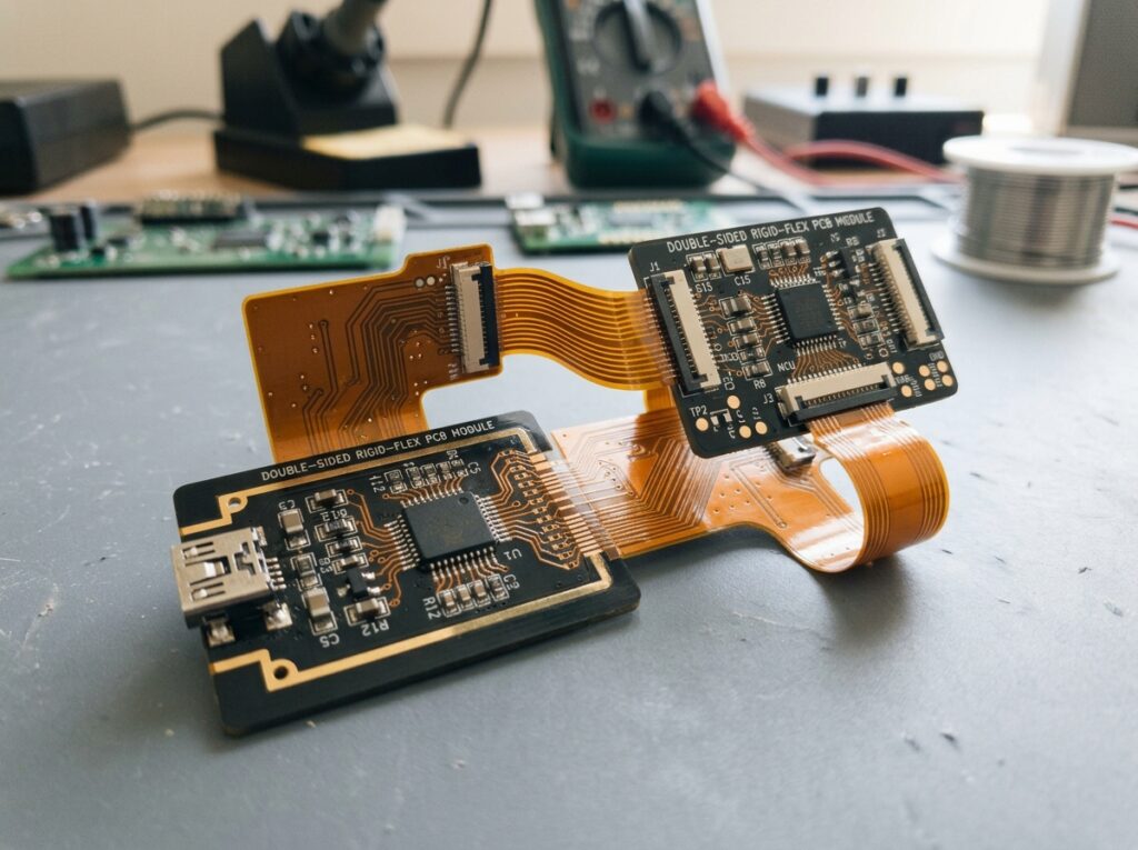
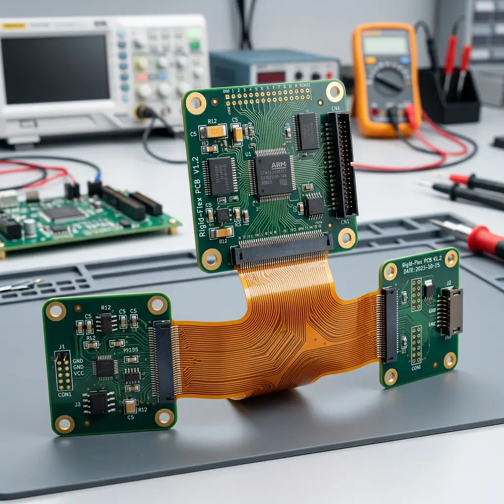
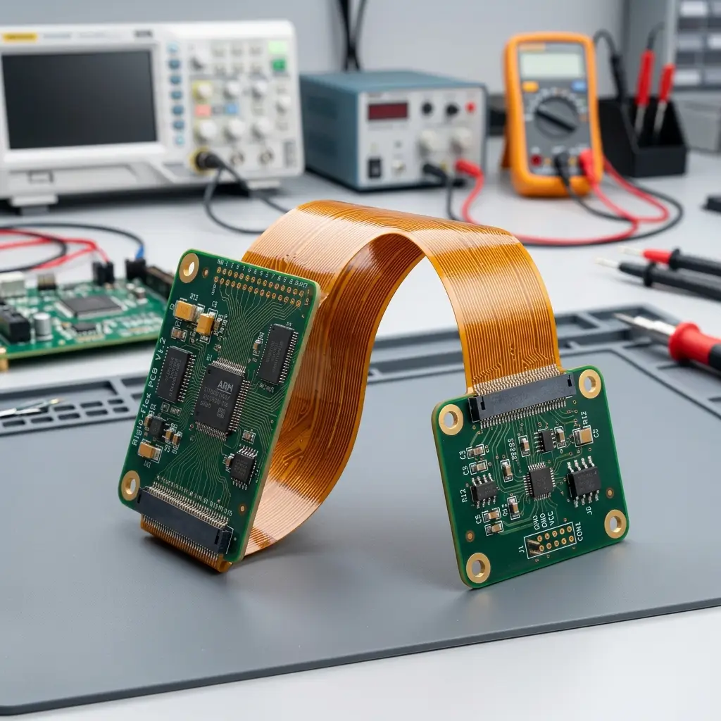
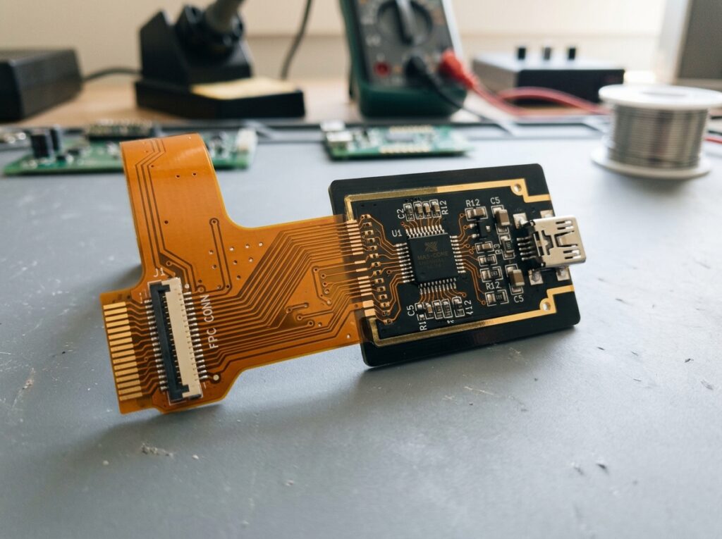
A rigid-flex PCB is a hybrid board that merges standard rigid substrate layers with flexible circuitry into a seamless, unified 3D assembly.

Key Advantages

  • Space and Weight Reduction: Eliminates bulky wires and connectors, shrinking the overall footprint in tight enclosures.

  • Higher Reliability: Fewer physical connectors and soldered joints mean fewer potential points of failure from vibration or mechanical stress.

  • 3D Design Freedom: Allows circuits to bend around corners, fold like origami, and fit custom or irregular 3D shapes.

  • Improved Signal Integrity: Consistent material properties and fewer interface transitions enhance electrical performance.

Why Choose Rigid-Flex PCBs

Topfast delivers high-reliability rigid-flex solutions that maximize performance in compact designs.

60% smaller than traditional boards with wiring harnesses

Bend and fold to fit complex geometries

100,000+ flex cycles with no connection failures

Withstands extreme temperatures up to 300°C

Core Advantages

  1. Extreme Space & Weight Savings: Enables 3D folding and eliminates interconnect connectors, reducing system footprint and reducing wiring weight by up to 60–70%.

  2. Superior Reliability & Shock Resistance: Replaces failure-prone solder joints and headers with continuous flex traces, resisting harsh vibration and mechanical impact.

  3. Optimized Signal Integrity: Continuous trace routing across layers ensures stable controlled impedance, lower insertion loss, and strong EMI shielding.

  4. Lower Total Cost of Assembly (TCO): Higher raw PCB cost is offset by reduced BOM component counts, simpler manual assembly, and zero risk of miswiring.

Rigid-Flex PCBs
Proven Case Study

What is rigid-flex PCB design?

Rigid-flex PCB design is the engineering process of combining rigid substrate sections with flexible circuit layers into a seamless, three-dimensional electronic assembly. As a leading rigid flex PCB manufacturer and trusted rigid flex PCB supplier, we integrate dynamic bendability with structural stability during the rigid flex PCB fabrication stage to eliminate bulky cables, headers, and discrete connectors. By optimizing stackup configurations and trace routing for rigid flex PCB (also referred to as flex rigid PCB or PCB rigid flex), this hybrid architecture allows engineers to significantly reduce total system footprint and enclosure weight while enhancing signal integrity, mechanical reliability, and vibration resistance in high-density applications.
Why Choose Topfast

Designed for Extreme Reliability in Space-Constrained Applications

Up to 60% Space Saving

Eliminates heavy wire harnesses and connectors, dramatically reducing enclosure dimensions and overall system weight.

100,000+ Dynamic Flex Cycles

High ductility Rolled Annealed (RA) copper prevents trace micro-cracking during constant bending.

Thermal & Chemical Durability

Withstands temperatures up to 300°C and harsh chemical disinfection without layer separation.

Rigorous DFM & Quality Control

100% AOI, E-testing, Microsection analysis, and TDR impedance testing before shipment.

Ready to Start Your Rigid-Flex PCB Project?

Upload your Gerber files today for a professional DFM review and detailed cost analysis within 24 hours.

Request a Quick Quote

Upload your Gerber files — DFM review & quote within 24 hours.

Engineering Capability

Technical Specifications & DFM Capabilities

ParameterMetric ValueImperial ValueFeature Highlights
Layer Count2 - 20 Layers2 - 20 LayersRigid-Flex Hybrid Stackup
Min. Core Thickness0.051 mm0.002″Ultra-thin Polyimide Core
Min. Trace / Space0.089 mm (3.5 mil)0.0035″High-Density Fine Line
Smallest Drill (Mech/Laser)0.18mm / 0.127mm0.0071″ / 0.005″Microvia / Blind & Buried Vias
Max Aspect Ratio10:110:1Reliable Plated Through Holes
Finished Copper WeightUp to 3 oz (89 μm)Up to 3 ozHigh Current Capacity
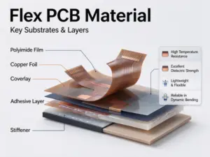
Flex Zone Stiffener0.1mm PI / Stainless / FR4Custom StiffenersOptimized Stress Relief

Premium Substrates & Surface Finishes

Surface Treatment Options

✔ HASL (Vertical or Horizontal)

✔ Lead-Free HASL

✔ OSP (Shikoku F2)

✔ OSP (Entek)

✔ ENIG (Electroless Nickel Immersion Gold)

✔ Immersion Silver

✔ Immersion White Tin

✔ Tin-Nickel

✔ Electrolytic Soft Gold

✔ Electrolytic Hard Gold

✔ Selective Gold

Surface Treatment Options


ParameterMetric ValueImperial Value
Min Core Thickness0.051 mm0.002″
Max Finished Copper Weight89 ml3 oz
Max Finished Copper Thickness0.009 mm–
Smallest Mechanical Drill0.180 mm0.0071″
Smallest Laser Drill0.127 mm0.005″
Min Finished Hole Size0.152 mm0.006″
Max Through Hole Aspect Ratio10:1–
Max Blind Via Aspect Ratio0.75:1–
Min Trace/Space (Rigid)0.089 mm0.0035″
Min Pad Size for Test0.127 mm0.005″
Material TypeExample / SubtypeFunction
ConductorsRolled Annealed (RA) CopperUsed in flexible circuits requiring repeated bending. It offers superior ductility, a grain structure aligned with the bend axis, and a reduced risk of micro-cracking.
Electro-Deposited (ED) CopperPreferred in rigid sections and some static flex zones. Provides high conductivity and fine trace definition but lower flex fatigue performance than RA copper.
AdhesivesEpoxyStrong adhesion with low moisture absorption. Tg typically ≥135 °C. Commonly used between copper and dielectric layers in rigid zones.
AcrylicHigh peel strength, chemical resistance, and thermal stability (Tg ~150 to 200 °C). Often selected for rigid-flex bonding interfaces.
Pressure Sensitive Adhesive (PSA)Low-temperature bonding layer is used to attach stiffeners or mount flex circuits. Limited to non-electrically active zones.
Polyimide (as adhesive)Extreme thermal resistance (>250 °C) and chemical durability. Used in aerospace-grade flexible PCB assemblies exposed to harsh environments.
Adhesiveless Base MaterialPolyimide is cast directly onto copper foil. Eliminates adhesive interface, improves flexibility, reduces Z-axis expansion, and enhances thermal reliability in dynamic flex circuits.
Pre-preg (Resin-coated Glass) Dielectric bonding sheet used during multilayer lamination in rigid areas. Properties depend on the resin system (Tg, flow, Dk/Df).
Insulators / DielectricsFR-4Standard rigid PCB core. Tg typically 135 to 170 °C. It provides mechanical support and a routing platform for rigid flex boards.
PolyimideHigh-flex, high-temperature material (Tg >250 °C). Used in flexible sections due to superior bend endurance and dimensional stability.
CEM-1Cellulose-based composite alternative to FR-4. Used in cost-sensitive rigid sections with low mechanical stress.
Polyester (PET)Flexible and thermally stable (~120 to 150 °C), lower cost than polyimide. Used in basic flexible PCB assemblies.
FAQ

Frequently Asked Questions

A rigid-flex PCB is a hybrid circuit board that seamlessly integrates rigid board sections (FR-4) with flexible substrate layers (Polyimide) into a single unified 3D assembly. It allows components to be mounted on rigid zones while flexible sections bend or fold to fit compact enclosures.

Rigid-flex PCB design is the engineering process of planning multi-layer stackups, signal routing, and transition zones between rigid and flex substrates to ensure electrical performance, thermal stability, and mechanical durability across static or dynamic bends.

  • Rigid PCB: Completely stiff, relies on external wire harnesses and connectors to join multiple boards.

  • Flex PCB: Thin and flexible throughout, designed for light weight and continuous dynamic flexing.

  • Rigid-Flex PCB: Combines both into one piece, eliminating connectors and wiring entirely for true 3D spatial folding.

A flex PCB with a rigidizer uses localized stiffeners (FR-4, aluminum) purely for mechanical support under SMT components or connectors without extra conductive layers. In contrast, a rigid-flex PCB features integrated multi-layer conductive circuits running continuously through both rigid and flex regions.

Rigid-flex PCBs eliminate bulky wire harnesses, reducing interconnect failure points, system weight, and volume. They provide superior resistance to shock and vibration, optimized signal integrity (controlled impedance), and lower total assembly labor costs.

We support customized rigid-flex PCB designs from 2 up to 20 layers, including complex HDI, blind/buried vias, and asymmetric rigid-flex stackups.

Key challenges include managing material expansion/contraction across dissimilar substrates (FR-4 vs. Polyimide), achieving precise layer registration during multi-stage lamination, controlling unbonded flex regions, and controlling thermal stress during soldering.

Please provide your Gerber files (including layer stackup and flex zone definitions), PCB quantity, surface finish requirement, copper weight, and stiffener specs.

Yes, upon request, we provide full quality verification reports including TDR impedance test reports, microsection analysis, and dynamic flex test data.

Our factories are ISO 9001, ISO 13485 (Medical Devices), ISO 14001, UL, and RoHS certified. All rigid-flex boards meet IPC-6013 Class 2 and Class 3 standards.

Overall board thickness varies depending on layer count and application:

  • Flex sections: Typically $0.002\text{ to }0.010\text{ inches}$ ($0.05\text{–}0.25\text{ mm}$).

  • Rigid sections: Standard thickness ranges from $0.016\text{ to }0.093\text{ inches}$ ($0.4\text{–}2.4\text{ mm}$), commonly $1.6\text{ mm}$ ($0.062\text{ inches}$).

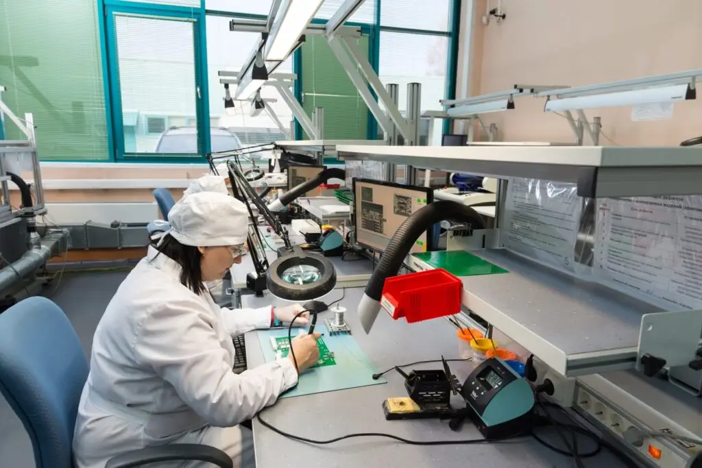
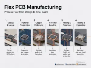
The manufacturing process involves preparing polyimide inner cores, etching flex circuits, applying polyimide coverlays, pre-assembling with FR-4 rigid layers, executing multi-stage lamination, laser/mechanical drilling, plating through-holes, and routing rigid outer contours.

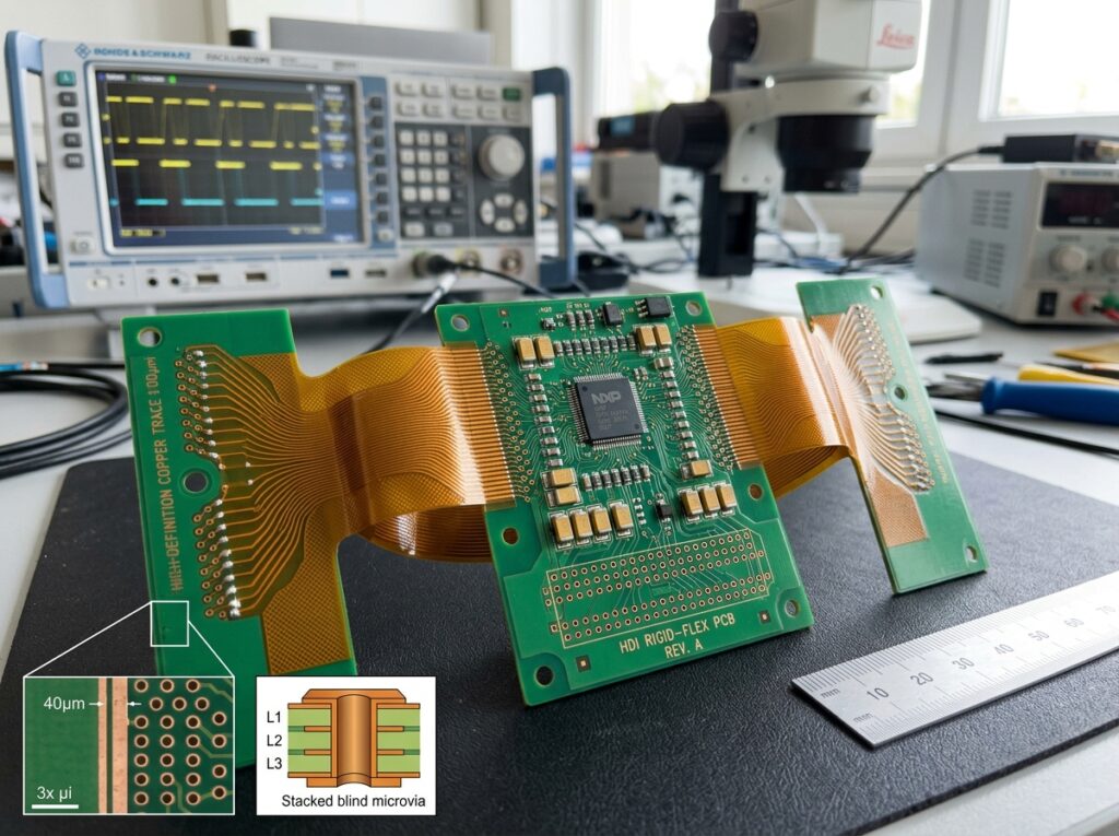
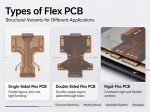
Common configurations range from single-sided flex with rigid stiffeners, traditional 4–12+ layer symmetrical stackups, embedded/flex-cap structures, air-gap unbonded flex layers for dynamic bending, to High-Density Interconnect (HDI) rigid-flex boards with laser microvias.

Key rules include avoiding vias/pads in flex transition bend zones, keeping copper traces perpendicular to bend lines, using teardrops on pads, maintaining a minimum bend radius ($10\text{–}12\times\text{ flex thickness}$ for dynamic flex), and using hatched copper planes instead of solid planes in flex zones.

Get Inquiry

Phone/Wechat

+86 18681608727

Email

vebesco@outlook.com

Phone/Wechat

+86 18681608727

Phone/Wechat

+86 18681608727