Almost every compact electronic product has a spot where a flat board will not fit: a hinge, a camera module that folds during assembly, a sensor that has to follow the curve of a housing. Rigid laminate cracks there, or it forces the designer to add a cable and two connectors. A flexible PCB removes that problem by making the interconnect itself the part that moves.
A flexible PCB is made by bonding copper foil to a thin polyimide or polyester film, imaging and etching the circuit into that copper, then laminating a flexible coverlay over the traces to insulate them. The steps look like rigid pcb manufacturing, but the base film is thin, dimensionally unstable under heat and humidity, and easy to crease, so drilling, plating, lamination and cutting all run with tooling and handling rules written for film instead of glass-reinforced laminate.
The rest of this guide goes through the process in the order a factory runs it, then answers the three questions buyers ask next: how thin the board can get, what sets the price, and what to hand a flexible PCB supplier before asking for a quote.
What makes a flexible PCB different from a rigid board
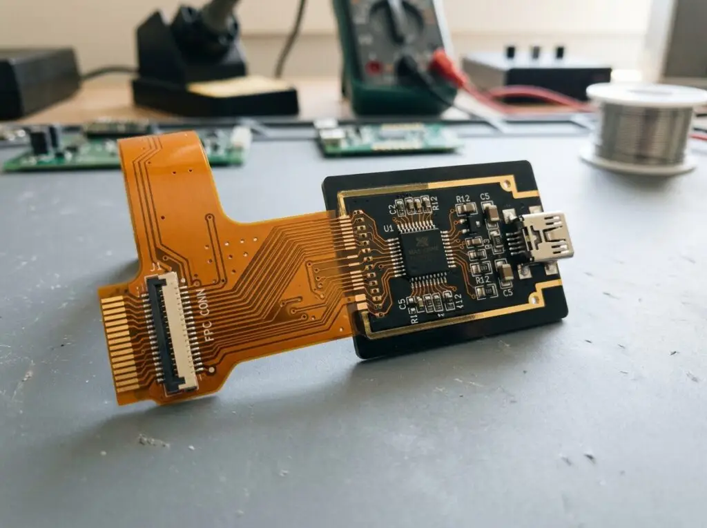
The difference starts with the base material and ends with what the assembly no longer needs. A rigid board uses glass-reinforced epoxy that holds its shape and carries heavy parts. A flexible pcb board uses a plastic film, so the circuit can fold once during assembly or flex continuously in service, and the connectors and wiring it replaces simply disappear.
That last point is where the real saving sits. A flex circuit joining two rigid boards across a hinge removes two connectors, a cable, and the labor to fit them. Fewer parts means fewer failure points, which is why flex turns up wherever vibration or repeated movement would otherwise kill solder joints.
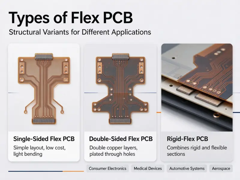
The standard that qualifies these boards, IPC-6013, sorts them by construction type: single-sided, double-sided with plated through holes, multilayer, rigid-flex, and multilayer constructions without through holes. It also sets performance classes and an installation-use class covering whether the board flexes once or continuously. A flexible pcb design can run from one conductive layer to well over ten, but more layers do not buy more bend life. Thicker stack-ups bend less, so layer count is a routing decision rather than a durability one.
The trade-offs are real: material costs more per unit area, the rules are stricter, and rework is harder once parts are mounted.
Which materials go into a flexible PCB
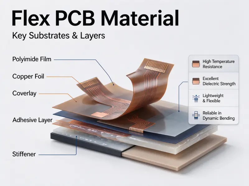
A flexible PCB is built from five things: a base film, copper foil, an adhesive system, a coverlay that protects the finished circuit, and often a stiffener under connectors or heavy parts. Each one is chosen against the bend requirement, not against cost alone.
Base film: polyimide and polyester
Polyimide is the default flexible pcb material. It survives reflow temperatures, resists most solvents, and holds its properties across a wide temperature range. Polyester costs less but will not take the heat of normal soldering, so it stays in low-temperature products such as membrane keypads.
Copper foil: rolled annealed or electrodeposited
Two copper types are used. Rolled annealed foil is made by rolling, so its grain runs in the rolling direction and gives better fatigue life under repeated flexing. Electrodeposited copper is cheaper and suits boards that fold once and then sit still. If you are early in the pcb learning curve, this is the decision most tied to whether a dynamic application survives its cycle count.
Adhesive, coverlay and stiffener
Adhesive bonds copper to film and coverlay to circuit. Adhesiveless constructions bond copper straight to the base film, giving a thinner board at higher material cost. The coverlay is a polyimide film with adhesive on one side, and it takes the place of solder mask, leaving openings where pads need to be exposed. Stiffeners are patches of polyimide, epoxy glass or metal bonded under a flexible pcb connector area or a heavy component.
| Layer | What it does | What drives the choice |
|---|---|---|
| Base film | Carries the circuit, sets bend behaviour | Temperature, cost, bend life |
| Copper foil | Forms the conductors | Static fold vs repeated flexing, current load |
| Adhesive | Bonds film to copper, coverlay to circuit | Thickness target, thermal exposure |
| Coverlay | Insulates and protects the traces | Pad openings, bend radius, abrasion |
| Stiffener | Adds local rigidity | Connector type, component weight |
| Surface finish | Keeps pads solderable | Shelf life, pitch, assembly process |
How a flexible PCB is made, step by step
The sequence is: prepare and dry the laminate, drill the holes, pattern the copper by imaging and etching, plate the holes, laminate the coverlay, apply the surface finish and stiffeners, then cut the profile and test. Every stage works the same in principle as rigid work. The difference is that the panel is a film that stretches, shrinks and creases if it is mishandled.
Step 1: design review and panel layout
Before any material is cut, the fabricator reviews the pcb board design against its process: bend zones, copper type, coverlay openings, stiffener positions and impedance requirements. Panels are laid out to get the most parts per sheet, since panel utilization is one of the two largest cost drivers.
Step 2: cutting, cleaning and drilling
Roll or sheet laminate is cut to panel size and baked to drive out moisture, which stabilizes the material before it sees heat. Holes are drilled mechanically or with a UV laser, depending on size. Polyimide smears when drilled, so a plasma or chemical desmear step cleans the hole wall before plating. Without it, copper will not bond to the hole reliably.
Step 3: circuit imaging and etching
A photoresist goes onto the copper, the circuit image is exposed onto it, and the unexposed resist is washed away. Chemical etching then removes the unprotected copper, leaving the pcb circuit pattern. Flex lines are finer than typical rigid lines, but etch control has to be tight: over-etching narrows traces, under-etching leaves shorts.
Step 4: via plating and hole metallization
Drilled holes get a thin electroless copper seed, then electrolytic copper builds the wall up to the specified thickness. Flex plating runs at lower temperatures than rigid plating, and the deposit has to stay ductile, because a brittle via wall cracks the first time the board bends.
Step 5: coverlay lamination
The coverlay is cut or laser drilled to create pad openings, aligned to the circuit, and bonded in a heated vacuum press. Alignment is the hard part: an opening that misses its pad by a fraction of a millimetre either blocks solder or leaves copper exposed. Some designs use a flexible liquid photoimageable mask instead, which gives finer openings at the cost of some bend performance.
Step 6: surface finish, stiffener and marking
Exposed pads get a finish that keeps them solderable through storage and assembly. Electroless nickel immersion gold is the usual choice for flex because it is flat and survives bending, while immersion tin and organic solderability preservative appear where cost matters. Stiffeners go on under controlled heat and pressure, then silkscreen is printed.
Step 7: profiling, electrical test and packing
Parts are separated from the panel by laser cutting, die cutting or routing, and laser is preferred where the outline is complex or the material is thin, since a die can pull or tear the film. Every circuit is tested for continuity and isolation, usually on a flying probe with soft contacts that will not dent the surface. Dimensional checks and visual inspection close out the build, with bend cycle testing added for dynamic applications.
How thick is a flexible PCB, and how far can it bend
Flexible pcb thickness is the sum of its layers, and a simple single-sided construction typically lands near 0.1 mm before finish and stiffeners. How far it bends is not a property of the material alone. It depends on total thickness, layer count, copper type, and whether the bend happens once or thousands of times.
The stack adds up quickly. This is an illustrative example, not a standard figure, to show where the thickness comes from:
| Layer | Example thickness |
|---|---|
| Polyimide base film | 25 µm |
| Adhesive | 20 µm |
| Copper foil | 18 µm |
| Coverlay film | 25 µm |
| Coverlay adhesive | 20 µm |
| Total | about 108 µm |
Real numbers come from your fabricator’s data sheet and your own stack-up drawing, and stiffener areas are thicker again.
Bend radius scales with that total. A circuit that folds once during assembly can be folded far tighter than one that flexes continuously, and the rules of thumb differ accordingly, from a few times the thickness for a static fold up to well over ten times for a part in constant motion. IPC-2223 is the design standard that covers how to set it, and the practical advice is to declare the bend type, the inside radius and the cycle count on the drawing. Traces should run along the bend axis rather than across it, and heavy copper is best kept out of the bend zone.
What drives flexible PCB price
Flexible pcb price is driven mostly by layer count and by how many parts fit on a production panel. Material, tolerances, testing and volume move the number after that, and the per-part cost of a flex circuit is usually higher than an equivalent rigid-flex board.
Comparing pcb price per part against a rigid board misses half the picture, though. A flex circuit that replaces a cable plus two connectors also removes the cost of buying, stocking and assembling them. The honest comparison is at the assembly level.
| Driver | What it does to cost | Where you have leverage |
|---|---|---|
| Layer count | Each layer adds a lamination cycle and lowers yield | Question whether the routing needs it |
| Panel utilization | Odd shapes and small tabs waste sheet area | Let the fabricator adjust the outline |
| Material system | Adhesiveless and specialty films cost more | Standardize unless the design needs otherwise |
| Feature size | Fine lines and small vias cut yield | Tighten tolerances only where needed |
| Copper type | Rolled annealed for dynamic flex costs more | Specify it only in bend zones that move |
| Testing | Bend cycle and impedance testing add time | Specify the cycle count you actually need |
| Volume | Tooling is amortized over the run | Prototype pricing is not production pricing |
The two items buyers can influence most are the outline and the layer count. A small tab on one edge can push a part off a panel row and raise the per-part cost noticeably, which is why early involvement from the flexible pcb manufacturer pays for itself.
Where flexible PCBs are used
Flexible PCBs turn up wherever something has to move, fold, or fit a shape a flat board cannot take. The largest volumes sit in consumer pcb electronics, and the strictest requirements sit in medical, automotive and aerospace work.
Consumer devices use them for camera modules, displays, hinges and battery connections. Medical designs use them in catheters, hearing aids and implantables that must stay small and reliable over a long life. Automotive work covers instrument clusters, sensor harnesses and lighting, where vibration would break solder joints on a rigid assembly. Aerospace uses them for weight saving and tight harness routing, and industrial equipment uses them in robotic joints and moving sensors.
What to send a flexible PCB manufacturer before quoting
Send the Gerber files, the stack-up you want, and a drawing that states the bend type, the bend radius and the expected cycle count. Those mechanical declarations are what a flexible pcb manufacturer prices against, and leaving them out is the most common reason a quote comes back with questions.
A complete package looks like this:
- Gerber or ODB++ data, plus a fabrication drawing with outline and tolerances.
- Stack-up: layer count, base film and copper thicknesses, adhesive or adhesiveless.
- Bend declaration: static fold or dynamic flexing, inside radius, cycle count, and where the bend zones sit.
- Coverlay openings and stiffener locations, with material and thickness.
- Surface finish and, if a zero insertion force connector is used, the connector type and required tail thickness.
- Electrical requirements: impedance targets, current loads, shielding.
- Quantity for both prototype and production, plus target lead time.
If you are unsure about any of these, say so in the request. A fabricator would rather fill in a blank than discover it after tooling.
FAQ
How long does a flexible PCB last in a dynamic bending application?
There is no single number, because life depends on copper type, total thickness, bend radius and how often the part moves. A single-sided polyimide circuit built for dynamic flexing can reach a very high cycle count, while the same design with electrodeposited copper at a tight radius fails sooner. For safety related or hard to service products, state the cycle count in the drawing and ask for bend testing to that number.
Can a flexible PCB be repaired or reworked?
It can, but with difficulty. The base film does not take repeated heat the way rigid laminate does, the traces are thin, and the coverlay has to be opened and patched rather than scraped. Most factories treat rework as a last resort, and the usual answer to a failed flex part is replacement.
When is a rigid-flex board a better choice than a flexible PCB?
Rigid-flex suits designs that need both: rigid sections to carry components and connectors, and flexible sections to do the bending, all in one part with no connectors between them. It is the usual answer when the assembly would otherwise need a stiffener under every component area. Expect a longer build and a higher unit cost than a plain flex circuit. For a closer look at that construction, see our page on rigid-flex PCB options.