Products keep getting smaller, and the space inside them gets stranger every year. A wire harness that fit five years ago now competes with a battery, a camera module, and a heat sink, and every crimp is a place where the assembly can fail. Most teams meet flex when they ask a flexible PCB supplier whether a fold, a hinge, or a curved housing can be wired without a bundle of cables.
A flexible PCB is a printed circuit board built on a thin, bendable polymer film instead of rigid fiberglass. Copper foil is bonded to that film, etched into traces, and sealed under a flexible coverlay rather than a liquid solder mask. It bends and folds into a three-dimensional space while carrying the same signals a rigid board would carry.
The sections below cover how it works, what it is made of, how the IPC standard classifies the types, how thin it gets, how it is built, what drives the price, and what to check before you pick a manufacturer.
How does a flexible PCB work?
A flexible PCB works like any other printed circuit: copper traces carry current and signals between components. The difference is mechanical. The base film lets the assembly move, so the board routes around a corner, folds into a stack, or flexes repeatedly through the life of the product.
The mechanical side is what separates a working design from a failed one. Copper work-hardens and cracks if you bend it enough times, and a cracked trace is an open circuit.
Static bending vs dynamic bending
IPC-6013D sorts flexible boards by installation use. Use A means the board withstands flexing during installation. Use B means it withstands continuous flexing for the cycle count written on the procurement documentation. Use C covers environments above 105 °C, and Use D covers applications that need UL recognition (IPC-6013D, checked 23 October 2026).
A board that folds once into an enclosure is a bend-to-install part. A board inside a laptop hinge, a print head, or a robot arm is a dynamic part, and it needs a symmetrical stack-up, annealed copper, and a larger bend radius.
What happens inside the bend
When a circuit bends, material on the outside of the curve stretches under tension and material on the inside compresses. In the middle of the stack there is a plane that sees neither, called the neutral bend axis (Flexible Circuit Technologies design guide, checked 23 October 2026). The further a layer sits from it, the more strain it takes, so keep the bend region thin, keep copper near the neutral axis, and keep vias out of the bend zone.
What is a flexible PCB made of?
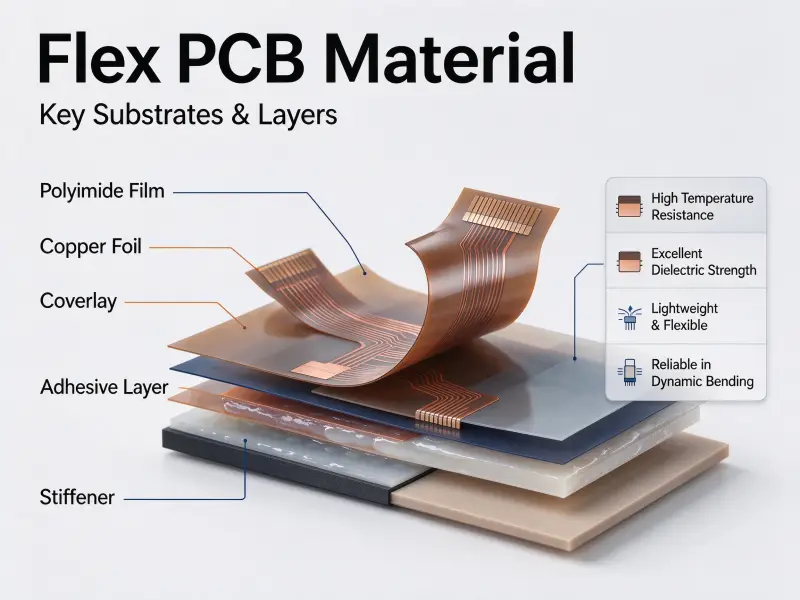
A flexible PCB is made of a flexible base film, a copper conductor layer, adhesive, a coverlay that protects the outer copper, and stiffeners where the board has to act like a rigid board. The combination sets how thin, how flexible, and how expensive the part is.
Base film
Polyimide is the default. It survives soldering temperatures, resists chemicals, and has a long bend life. Polyester, usually PET, costs less but has lower heat resistance, and liquid crystal polymer is used when the design needs low moisture absorption or stable high-frequency performance. Base film runs from 12 µm to 125 µm, or 0.5 mil to 5 mil, and thinner film bends more easily (Ansys, checked 23 October 2026).
Copper foil
Rolled annealed foil is rolled and then annealed, which elongates the grain structure in the plane of the foil and makes it more ductile. Electrodeposited copper is cheaper and is often used for thin foils and static applications. Copper weight is quoted in ounces per square foot, and flex constructions commonly run from 1/3 oz to 2 oz (Epec Engineering Technologies, checked 23 October 2026). Heavier copper carries more current and stiffens the bend.
Adhesive and coverlay
The coverlay is the flex equivalent of solder mask: a polyimide or polyester film coated with thermoset adhesive, usually epoxy or modified acrylic, laminated over the outer copper, with openings that are drilled, routed, or laser cut. Adhesive thickness has to fill around the traces, so copper weight and adhesive thickness are chosen together. Adhesiveless constructions are thinner and handle heat better, at a higher material cost.
Stiffeners
A stiffener is rigid material bonded to a region that must not bend. FR4 goes under components, polyimide stiffeners add local thickness, often to hit the insertion thickness a ZIF connector expects, and stainless steel or aluminum is used where the region needs rigidity or heat spreading.
| Layer | Material options | Typical thickness | Job |
|---|---|---|---|
| Base film | Polyimide, PET, LCP | 12–125 µm (0.5–5 mil) | Carries the circuit, sets flexibility |
| Copper | Rolled annealed or electrodeposited | 1/3 oz to 2 oz | Conducts current and signals |
| Adhesive | Epoxy or modified acrylic | 12–50 µm (0.5–2 mil) | Bonds foil to film and coverlay to circuit |
| Coverlay | Polyimide or polyester film | 12–50 µm (0.5–2 mil) | Insulates and protects outer copper |
| Stiffener | FR4, polyimide, stainless steel, aluminum | Set by the connector or component | Makes a local region rigid |
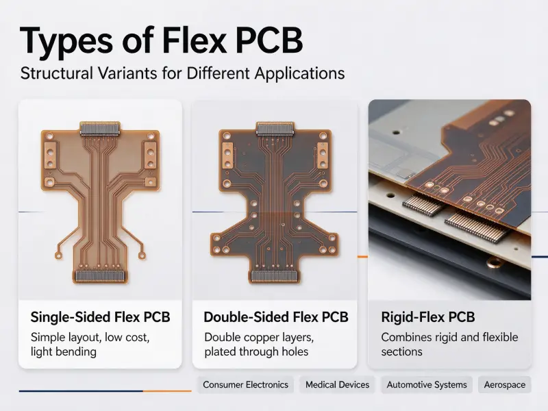
What types of flexible PCB are there?
IPC-6013D defines five types of flexible printed board, sorted by how many conductive layers the board has and whether plated through-holes connect them: Type 1 single-sided, Type 2 double-sided with plated holes, Type 3 multilayer, Type 4 rigid-flex, and Type 5 two or more layers without plated holes (IPC-6013D, checked 23 October 2026).
| Type | Construction | Typical use |
|---|---|---|
| 1 | One conductive layer, with or without stiffeners | Simple interconnects, bend-to-fit wiring |
| 2 | Two conductive layers with plated through-holes | Most common build, routing on both sides, controlled impedance |
| 3 | Three or more conductive layers with plated through-holes | Dense routing, high-speed buses |
| 4 | Multilayer rigid and flexible combination, three or more layers with plated through-holes | Replaces board-to-board connectors and cables |
| 5 | Two or more conductive layers without plated through-holes | Cost-sensitive designs that can avoid through-holes |
The standard, including performance classes and installation uses, is published by IPC at IPC-6013D.
Single-sided, double-sided, and multilayer flex
Single-sided flex is the simplest build: one copper layer on the base film, coverlay on top. Double-sided flex puts copper on both sides and connects them with plated through-holes, roughly doubling the routing in the same footprint. Multilayer flex stacks three or more conductive layers with flexible insulation between them. Every added layer buys routing density and costs flexibility, so multilayer flex is usually bend-to-install.
Flex vs rigid-flex
Rigid-flex is the Type 4 build. Rigid laminate sections and flexible polyimide layers are bonded in one pressing cycle, and the flexible layers run continuously through the rigid zones, so there is no connector and no solder joint at the transition. The trade-off is engineering time: the stack-up has to be designed as one part, and the drawing has to define the rigid zones, the flex zones, and the transition. Teams that need structural support and folding usually bring in a rigid-flex PCB manufacturer during layout rather than after it.
How thick is a flexible PCB?
A flexible PCB runs about 0.05 mm thick for a simple single-sided circuit and over 1.5 mm once you add layers, stiffeners, and shielding. Most of the thickness comes from layer count and stiffeners, not from the copper.
| Parameter | Typical range | Note |
|---|---|---|
| Base film | 12–125 µm (0.5–5 mil) | Thinner film bends more easily |
| Copper weight | 1/3 oz to 2 oz | Heavier copper stiffens the bend |
| Total circuit thickness | 0.05 mm to over 1.5 mm | Includes substrate, copper, and insulation (PCB Directory, checked 23 October 2026) |
| Two-layer flex, typical | About 0.11–0.25 mm (4.4–10 mil) | One supplier’s published typical range, checked 23 October 2026 |
| Stiffener thickness | Set by the connector or component | ZIF connectors often specify it |
How thickness sets the bend radius
Bend radius is the smallest radius the circuit can take without damage, quoted as a multiple of total thickness. Figures published by flex fabricators working to IPC-2223 design guidance put the minimum at roughly 6x the thickness for single-sided, 10x for double-sided, and 20x or more for multilayer (checked 23 October 2026). Dynamic applications need more than the minimum.
How is a flexible PCB manufactured?
A flexible PCB is built with the same imaging, etching, and lamination steps as a rigid board, plus three operations rigid boards don’t need: coverlay lamination, stiffener attachment, and, for rigid-flex, bonding rigid and flexible layers in one press cycle.
- Design and DFM review. Bend zones, stack-up symmetry, teardrops, and cross-hatched reference planes get settled before tooling.
- Material preparation. Thin films move and tear, so panels are handled on carriers or rigid fixtures.
- Drilling and via formation. Mechanical drilling for through-holes, laser for microvias, then copper plating.
- Imaging and etching. The pattern is photoimaged, developed, and etched.
- Coverlay lamination. Openings are cut, then the coverlay is aligned and pressed.
- Stiffener and shield attachment. FR4, polyimide, or metal stiffeners are laminated or attached with pressure-sensitive adhesive. EMI shielding films go on here too.
- Surface finish. ENIG, OSP, immersion silver, or immersion tin.
- Electrical test and inspection. Continuity and isolation testing, optical inspection, dimensional checks.
- Assembly. Components go on with fixtures that hold the circuit flat through reflow, or with conductive adhesive where soldering is impractical.
Where flex fabrication differs from rigid fabrication
Thin material moves during lamination, so registration tolerances are tighter and dimensional stability is a real process control problem, and coverlay openings have to align with pads on a substrate that can stretch. Rework is destructive, because reaching a trace means pulling the coverlay off and putting it back.
Where are flexible PCBs used?
Flexible PCBs are used wherever a rigid board cannot fit, cannot survive the motion, or adds too many connectors. The largest volumes run through consumer electronics, medical devices, automotive electronics, aerospace, and industrial equipment.
| Industry | What the flex circuit does | Why flex rather than rigid |
|---|---|---|
| Consumer electronics | Connects displays, camera modules, and hinges | Fits thin, curved space |
| Medical | Wearable sensors, hearing aids, catheters, implantable leads | Low mass, conforms to the body |
| Automotive | Clusters, cameras, lighting, sensor wiring | Handles heat and vibration |
| Aerospace and defense | Avionics, satellites | Cuts weight and removes connectors |
| Industrial | Robotics, moving print heads, inspection equipment | Survives repeated flexing |
What are the advantages and limits of flexible PCBs?
A flexible PCB saves space and weight and removes interconnection points, but it costs more to engineer, is harder to rework, and has size limits that rigid boards don’t.
Advantages
Flex circuits replace hand-built wiring with a repeatable automated assembly, which cuts wiring errors. Dropping connectors and cable assemblies drops failure points, and a flex circuit weighs less than the rigid board and harness it replaces while absorbing vibration and shock better. It also allows three-dimensional packaging, so the electronics follow the shape of the product.
Limits
Engineering cost comes first. Most flex circuits are custom, so artwork, phototools, and process setup get paid for before the first board exists. Rework is slow and risky, and panel size limits how large one piece can be. Handling during assembly damages circuits that rigid boards shrug off, and not every board house runs flex.
How much does a flexible PCB cost?
There is no standard price for a flexible PCB. The price follows the stack-up: layer count, base material, copper weight, coverlay and stiffener count, tolerances, test coverage, quantity, and lead time. Two boards that look similar on a drawing can price very differently.
| Cost driver | What moves the number | Effect |
|---|---|---|
| Conductive layers | Each layer adds lamination, drilling, and plating | Up |
| Base material | Polyimide, PET, or LCP; adhesive or adhesiveless | Up |
| Copper weight and type | Rolled annealed costs more; heavy copper costs more | Up |
| Coverlay, stiffeners, shielding | Extra pieces and extra alignment steps | Up |
| Bend class | Dynamic flex needs a symmetrical stack-up and annealed copper | Up |
| Tolerances and impedance control | Tighter control means more test and more scrap | Up |
| Quantity | Engineering cost spreads over the run | Down per unit |
| Lead time | Quick-turn compresses the schedule | Up |
Send a drawing package that states layer count, base material, copper weight and type, bend class with cycle count if the application is dynamic, finished thickness, quantity, and target lead time. The quote comes back itemized, and any change to the stack-up moves it.
How do you choose a flexible PCB manufacturer?
Choose on process capability first and engineering support second. The question isn’t whether a manufacturer can build a flex circuit, it’s whether they can build your construction, at your bend class, at your volume.
- Ask which IPC-6013 types and performance classes they run in production, not only in prototype.
- Check that they return DFM feedback before tooling: bend radius, stack-up symmetry, teardrops, cross-hatched planes.
- Check test coverage and traceability: electrical test on every net, impedance reports, lot traceability on materials.
- Ask about panel size limits, because they set the maximum size of one piece.
- Ask how prototype and production relate, since a prototype built on a different process tells you less than it looks like it does.
FAQ
What connector is used with a flexible PCB?
Zero insertion force connectors are the common answer. The flex circuit ends in a tail, a polyimide stiffener sets the tail thickness the connector expects, and the connector clamps it in place. Board-to-board connectors on a stiffened region and soldered tails landing on a rigid board are the other options. Connector and stiffener are usually chosen together, since both follow the same thickness requirement.
Can a flexible PCB be repaired or reworked?
Sometimes, but it isn’t cheap. Reaching a trace means removing the coverlay over it, doing the repair, and laminating new coverlay material. Thin copper lifts and tears easily, and a second reflow cycle on an assembled flex circuit risks joints you didn’t touch. Many factories replace the part rather than rework it, which is why test access matters more on flex than on rigid boards.
How long does a flexible PCB last in a dynamic application?
There isn’t a single number, because flex life depends on bend radius, copper type, stack-up symmetry, cycle count, and operating temperature together. What you can do is specify it: state the cycle count on the drawing under IPC-6013 Use B, and ask the manufacturer to validate the construction with a bend test on your stack-up. A dynamic design with no cycle count is a design nobody has tested.