Most HDI enquiries arrive at an HDI PCB manufacturer as a set of Gerbers and one line about needing a denser board. There’s a 0.4 mm pitch BGA on it, the outline is small, and the traces won’t route on a standard multilayer build. Three suppliers quote, and the prices differ without explanation.
A manufacturer worth ordering from can show you, on paper, which microvia structures it drills, how many sequential lamination cycles it runs, what line width and spacing it holds on inner versus outer layers, and how it verifies microvia reliability. Claims about advanced HDI capability are cheap. A stack-up review, a fabrication drawing, and test data are not.
Here is what to check, in the order a quote reaches your desk.
What qualifies a board as HDI
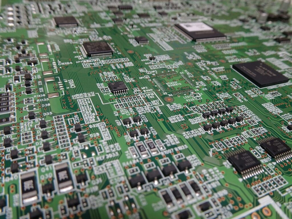
HDI is a geometry class you can measure. Under IPC-2226, a board counts as high-density interconnect when its microvias are 150 µm or smaller, land on capture pads of 350 µm or smaller, hold an aspect ratio near 1:1, and carry traces and spaces around 0.10 mm or finer.
The IPC-2226 sectional design standard is where those numbers come from. A microvia is a blind hole, laser or mechanically drilled, that terminates on a target pad within a capped depth. That cap is why they plate reliably.
| Parameter | IPC-2226 threshold | What it changes at the fab |
|---|---|---|
| Microvia diameter | 150 µm (about 6 mil) or less | Laser drilling: mechanical bits at this size deflect |
| Capture pad | 350 µm or less | Drives registration and layer-to-layer alignment |
| Aspect ratio | Around 1:1, ideally lower | Caps dielectric thickness per build-up layer |
| Trace width and spacing | 0.10 mm (4 mil) or finer | Thin foil, and at the low end semi-additive processing |
The four numbers to read first
Look for minimum laser-drilled via, minimum capture pad, minimum inner-layer line and space, and maximum microvia aspect ratio. A shop that drills 75 µm vias but holds 100 µm lines has lamination it can’t route to. The weakest figure sets your limit.
Why layer count doesn’t make a board HDI
A 12-layer board with plated through holes running surface to surface isn’t HDI, whatever the stack height. Two boards with identical layer counts can differ several times over in routable connections per square centimetre, and the HDI PCB price difference usually tracks routing density, not layer count. It’s the first correction to make when you start HDI PCB learning.
The via structures behind an HDI quotation
Every HDI quote is really a quote for a set of via structures. Through holes, blind vias, buried vias, laser microvias, stacked and staggered microvias, skipped vias and via-in-pad cost different amounts to produce, and mixing them wrongly is the most common reason a first article fails.
A through hole crosses the whole board and eats routing space everywhere. A blind via starts on a surface and stops inside. A buried via connects inner layers only. The last two hand surface space back to fine-pitch parts.
| Via type | Formed by | Reaches | Where it earns its cost |
|---|---|---|---|
| Plated through hole | Mechanical drill, full board | All layers | Connectors, power entry, Type I core interconnect |
| Blind via | Mechanical or laser drill | Surface to inner | Freeing routing near dense parts |
| Buried via | Drilled before outer lamination | Inner layers only | Inner interconnect with clean surfaces |
| Microvia | Laser, one dielectric layer | One layer pair | Fine-pitch fan-out, high pad density |
| Stacked microvia | Aligned laser drills, copper-filled between | Two or more layer pairs | Vertical path through a build-up |
| Staggered microvia | Offset between layers | Two or more layer pairs | Same reach as stacked, no fill step |
| Skipped via | One laser drill through two dielectrics | Two layer pairs | Drops an intermediate landing pad |
| Via-in-pad | Microvia inside the pad | One layer pair | Decoupling loops, BGA escape |
Microvias, blind vias and buried vias
The commercially important distinction is drill method. Mechanical drilling below roughly 0.15 mm is slow and hard on tooling, so most shops set a floor near there and switch to laser. Laser drilling leaves a conical hole with a heat-affected rim, which is why capture pad and dielectric thickness are specified together. Ask which method the shop plans for each via class.
Stacked, staggered and via-in-pad
Stacked microvias give a straight vertical path and the hardest build: each via needs filling and planarisation before the next press. Staggered microvias skip the fill by offsetting each layer, at the cost of lateral space. Via-in-pad fails in a specific way: an unfilled via in a landing pad wicks solder down the barrel during reflow and starves the joint.
Reading a stack-up: what 1+N+1 commits you to
The build-up notation tells you how many lamination cycles the shop must run, and that number drives yield and cost. 1+N+1 means one microvia layer per side. 2+N+2 means two per side and two sequential passes. Any-layer means no core, with a laser-drilled layer pair almost everywhere.
The N is the core, usually a conventional multilayer board with plated through holes. Everything outside it is build-up, added in its own press cycle, then drilled, plated and inspected.
| Build-up | Microvia layers per side | Lamination cycles | Common total layers | Fits |
|---|---|---|---|---|
| 1+N+1 | One | One build-up cycle | 4 to 8 | Consumer devices, industrial controllers |
| 2+N+2 | Two | Two sequential cycles | 8 to 12 | Automotive modules, denser BGA fan-out |
| 3+N+3 | Three | Three sequential cycles | 10 to 16 | High pin-count processors, compact modules |
| Any-layer | Every layer pair | One per layer pair | 8 and up | Phone-class boards, package substrates |
Each build-up layer is another chance to lose registration
Every press cycle lets the dielectric move a little, and every laser drill has to hit a pad defined two processes earlier. Ask for the layer-to-layer tolerance on a build-up layer, not on the core. That figure decides whether a 0.4 mm pitch device escapes cleanly.
Where rigid-flex HDI fits
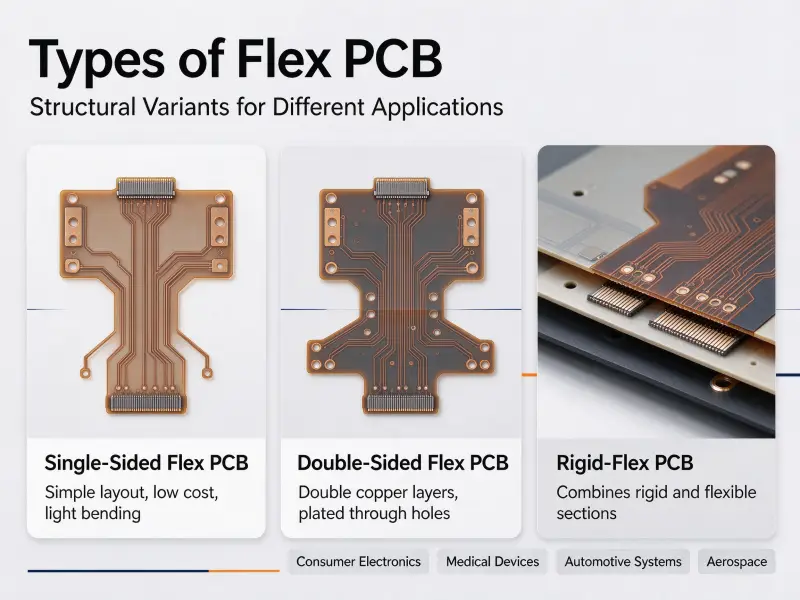
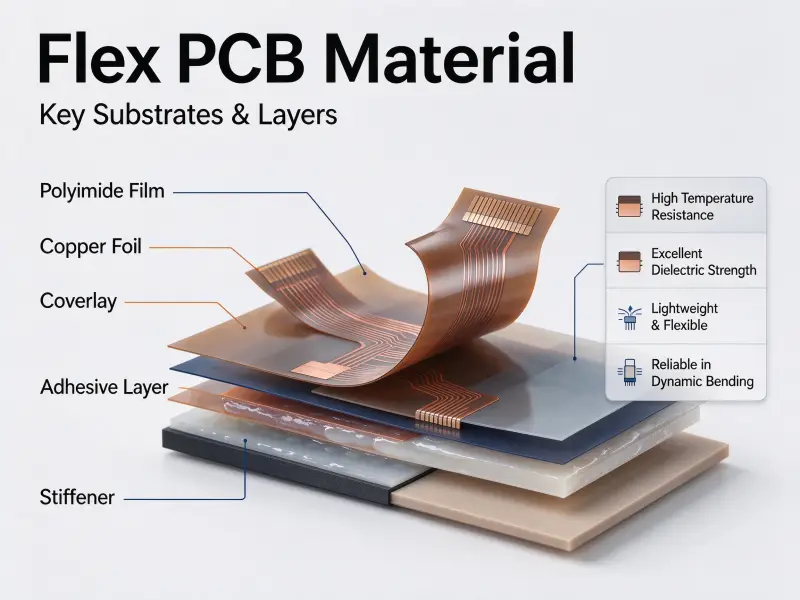
Build-up technology doesn’t stop at rigid boards. A rigid-flex PCB can carry microvias in its rigid sections while the flexible sections stay thin enough to bend, which is how many camera modules are built. The flexible core constrains lamination temperature and pressure, so the build-up schedule has to be settled before the stack-up is frozen.
How HDI changes what happens on the fabrication floor
HDI moves the difficulty from imaging to handling. Fine lines are the visible change. The harder problems are laser drill energy control, thin dielectric handling, copper fill of small holes, and keeping every layer aligned through two or three press cycles.
Start with the dielectric. A build-up layer is typically 60 to 100 µm of prepreg, sometimes less. That thinness keeps the microvia aspect ratio near 1:1, but it leaves the press little margin for resin flow, and thin cores warp. Warpage reappears as placement error at assembly.
Then copper. Fine lines need foil of 9 to 12 µm, because thick copper undercuts during etching. Below roughly 50 µm, many shops switch to semi-additive processing, plating the conductor up instead of etching it down, which means a different line and cost base. Plating caps the sequence: at 1:1 the solution still exchanges at the bottom of the hole, and past that the barrel plates thin, passes test, and fails in the field. Materials follow the same logic. Multiple reflow passes call for a glass transition temperature around 170°C or above; high-speed designs let dielectric constant and loss tangent pick the material, which then picks the stack-up.
What a capable HDI supplier can show you
Ask for capability data in writing, then ask how it’s verified. A shop that builds HDI in-house answers both without hesitation. A shop that brokers it answers the first and deflects the second.
Most of these items appear on any capability sheet. What matters is the document behind the number when you ask for it.
| Question | Why it decides the job | Warning sign |
|---|---|---|
| Maximum sequential lamination cycles | Caps the build-up you can specify | A number below your stack-up |
| Minimum laser via and aspect ratio | Sets the smallest microvia held in production | Prototype figures quoted as production limits |
| Inner and outer line/space | The inner figure is usually the tighter one | One number quoted for both |
| Drilling and lamination in-house | Determines who controls yield | Vague talk of partner factories |
| Microvia fill method | Copper and epoxy fill behave differently under cycling | No answer on fill, only “we do via-in-pad” |
| Impedance verification method | Coupon data beats a claimed tolerance | A tolerance with no test coupon mentioned |
Process control and inspection evidence
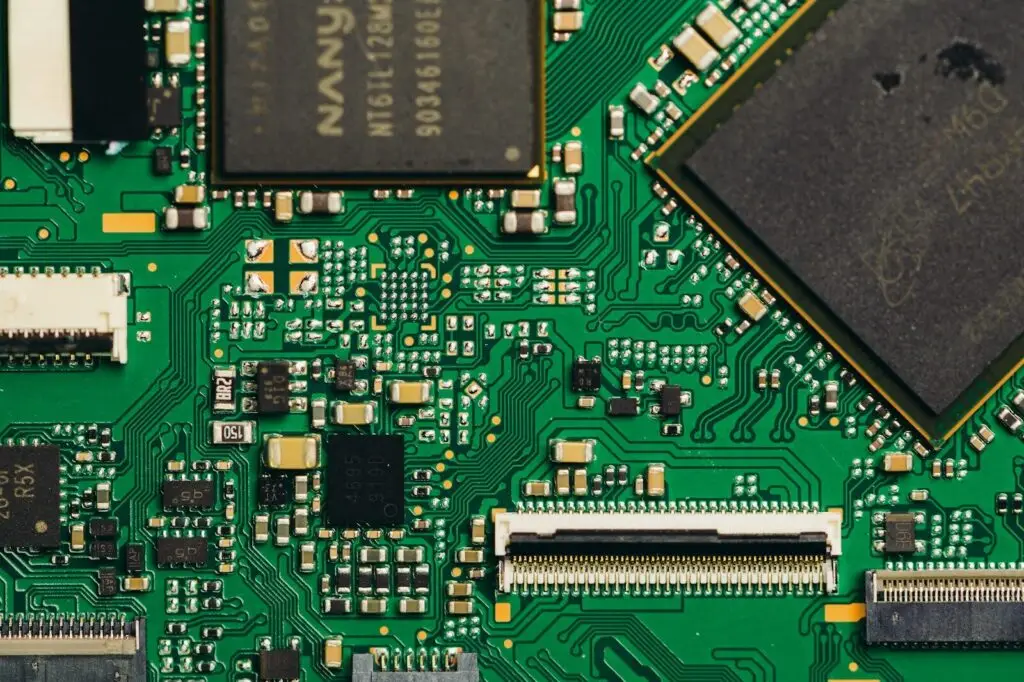
Optical inspection catches surface defects on each layer before lamination. X-ray catches registration and voids in buried structures. Cross-sectioning on a first article confirms barrel thickness and fill. Electrical test catches opens and shorts but not a marginal barrel, which is the failure that reaches the customer. Ask whether you get a copy of that report.
Red flags in the RFQ conversation
Two things should end a conversation. A quote with no question about the stack-up means nobody read the design. A price far below the others usually means microvias were priced as mechanical blind vias, which cost less and fail differently.
Where HDI cost actually come from
HDI has no standard price multiplier. Cost comes from cycle count, microvia count, fill steps, material grade and yield, and those five move independently. A single build-up with a few hundred microvias can cost less than a two-layer build-up of the same layer count.
| Cost driver | Why it adds cost | Where you can pull it back |
|---|---|---|
| Lamination cycles | Each is a press, drill, plating pass and inspection | Drop a build-up if routing still closes |
| Microvia count and density | Drill time, per-hole inspection | Rework the fan-out before release |
| Stacked versus staggered | Stacked needs fill and planarization between layers | Use staggered where the offset fits |
| Laminate grade | High-frequency and high-Tg materials process slower | Specify only the grade needed |
| Panel utilisation | Tight arrays waste panel area | Resize the array and rails before quoting |
Fix design rules first and treat price as an output. A microvia removed in design review costs less than one negotiated at quotation.
Design decisions that decide buildability
Most HDI boards that fail at fabrication were decided in layout, not in the fab. Via-in-pad fill, fan-out geometry and reference-plane continuity are worth reviewing before release.
Via-in-pad needs a fill spec
“Via-in-pad” on a drawing is incomplete. Say whether the via is filled with copper or epoxy, whether it’s capped and plated over, and what flatness assembly needs. Copper fill and planarisation give the flattest surface and the best thermal path. Epoxy is cheaper and fine for many designs, but it must be fully cured and planarised, or the pad sits proud and the stencil deposit goes wrong.
Fan-out and reference planes
A 0.4 mm pitch BGA gives roughly two trace channels between adjacent pads on one layer, before via lands are counted. Dog-bone fan-out burns the space you just bought, and via-in-pad only recovers it if the capture pad and mask clearance still work at that pitch. Do that calculation before choosing the build-up. Keep the return path in mind too: a microvia that breaks a reference plane creates an impedance discontinuity, so add stitching vias where a signal via changes reference.
Assembling the RFQ package
A good HDI RFQ is a small document set, and every item in it removes a question the fabricator would otherwise answer with an assumption.
- Gerber or ODB++ data, with the drill file split by via class rather than merged.
- A stack-up drawing with material, dielectric thickness and copper weight per layer.
- The build-up type requested, written as 1+N+1 or 2+N+2, or a request to propose one.
- An impedance table with target value and tolerance for each controlled line.
- A fill and capping requirement, stated per via class.
- The acceptance standard and IPC class, plus any application-specific requirement.
- Inspection and test requirements, including whether you want first-article cross-sections.
- Quantities across prototype, pilot and production, since panel utilisation changes with volume.
Send the same package to every supplier you compare. A quote that comes back materially lower usually reflects how the package was read.

FAQ
Can an existing through-hole design be converted to HDI without a redesign?
Not as a file conversion. A through-hole layout reserves via land space on every layer, and that space disappears once the vias move. A partial conversion works: keep plated through holes in the core, re-route the dense areas with microvias, then re-check the stack-up and impedance.
Is any-layer HDI the same as 2+N+2?
No. The N in 2+N+2 is a core, so the board keeps mechanical through holes in the middle and two build-up layers per side. Any-layer has no core in that sense: every layer pair is laser-drilled, which allows a via anywhere at the cost of more press cycles.
How are microvias under component pads inspected?
Optical inspection can’t see them once the pad is covered, and X-ray shows a barrel poorly through copper fill. Cross-sectioning on a first article shows barrel thickness and fill; thermal cycling on coupons shows whether the process holds. Ask for both.