Radar front ends, flight computers, and satellite payloads now carry fine-pitch BG. As a conventional multilayer board cannot route without extra layers and weight. The board has to get denser without getting bigger, and it has to survive vibration, vacuum, and thermal cycling for the life of the platform. That combination is why shortlists for an HDI PCB board manufacturer start with process capability rather than price per square meter.
HDI PCB for aerospace and defense is a high-density interconnect board built with laser-drilled microvias, blind and buried vias, and fine line-and-space geometry, then qualified to IPC Class 3 workmanship and documented for traceability. The density is the easy part to describe. The hard part is proving those microvias survive the thermal and mechanical life of the platform.
The sections below cover what HDI changes inside the board, how the build sequence runs, and what to check before a lot ships.
What HDI means for a PCB
HDI stands for high density interconnect. An HDI board uses microvias and fine features to route more connections in less area than a standard multilayer board allows. In IPC terms, a microvia is a blind via with an aspect ratio of 1:1 or less and a depth of no more than 0.25 mm, which is why it gets laser drilled rather than mechanically drilled.
A mechanically drilled blind via 0.3 mm deep is not a microvia, so the definition is worth pinning down at quoting time. Three via structures do the work:
- Microvia. Laser drilled, reaches one adjacent layer, typically 75 to 100 µm across in production.
- Blind via. Connects an outer layer to an inner layer without crossing the board.
- Buried via. Connects inner layers only, so it is finished before the outer layers go on.
The three HDI types, and what each one buys you
IPC-2226 sorts constructions by how many microvia layers sit on each side of the core, and whether the core carries buried vias.
| Type | Notation | Build-up | Where it fits an aerospace program |
|---|---|---|---|
| Type I | 1[C]0 or 1[C]1 | One microvia layer per face | Control cards with first-inner-layer escapes |
| Type II | 1[C]0 or 1[C]1 plus buried vias | Single build-up, buried vias in core | Inner routing through-holes would choke |
| Type III | 2[C]2, 3[C]3 and up | Two or more layers per side | Radar modules, FPGA carriers |
| Any-layer | Every layer laser drilled | Stacked microvias, no core | Tightest weight budgets |
Most programs that ask for HDI need Type I or Type II. Type III and any-layer add press cycles, and press cycles add cost and yield risk. Pick the type from the escape the package needs, then put the stackup and via map on the drawing. Most HDI PCB design mistakes start with a type chosen for its label rather than the escape it has to serve.
Why avionics and defense programs move to HDI
The move is usually forced by package pitch and by space. When a fine-pitch BGA has to escape inside a board outline fixed by an enclosure or a payload envelope, plated through-holes block the channels underneath the array. HDI is the standard way out of that corner.
A 0.5 mm pitch array leaves roughly a quarter of a millimeter between ball centers, and a through-hole with its pad and clearance eats most of that. Drop to a microvia on the first inner layer and the outer rows route on the surface while the rest fan out below.
Weight and volume, not only routing density
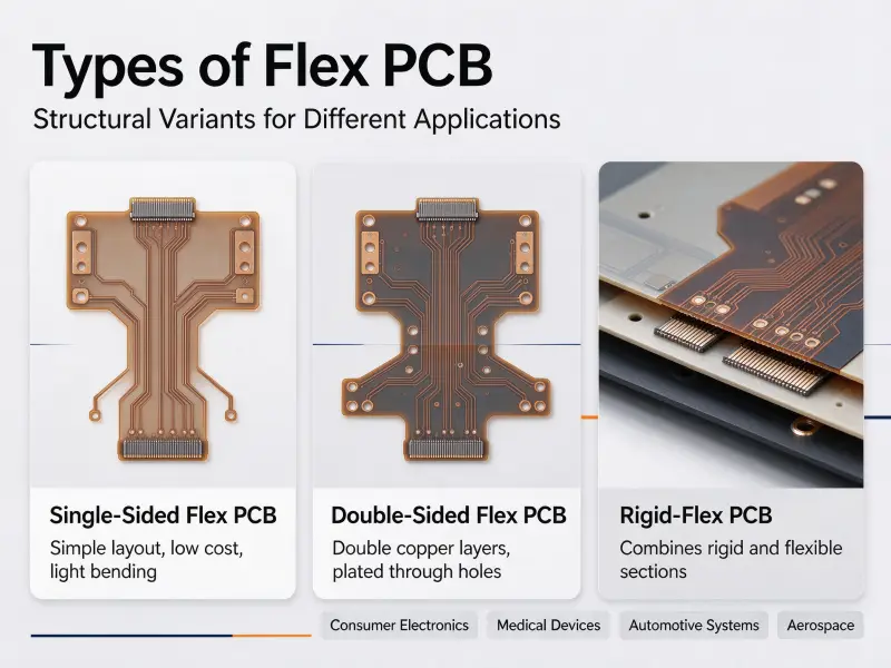
Fewer layers for the same net count means a thinner board and a lighter card cage. Where the harness itself is the problem, a rigid-flex PCB folds the interconnect into the board and removes connectors, cable runs and the labor of routing them. Both moves trade manufacturing complexity for system-level savings, so settle them before the enclosure is frozen.
Stackup and via choices that set reliability
Layer count tells you how much routing room a board has. Lamination cycles tell you how much risk it carries. Every build-up layer adds a laser drill, a desmear step, a plating step and a press cycle, and each one is a place where a microvia can end up with a thin wall, a void or a poor capture land.
Aerospace and commercial programs diverge most here. A consumer board can absorb a small fallout rate at final test. A board that flies cannot, because the failure that matters is the microvia that passes test and cracks after a few hundred thermal cycles. Plating quality, resin fill and interface condition decide that outcome, and none of it shows up in a visual inspection.
Stacked versus staggered microvias
Class 3 practice is to stagger microvias wherever routing allows, because strain spreads across separate layers instead of concentrating in one vertical copper column. When a design does stack, two levels is the usual ceiling before a qualification plan has to justify more.
Via-in-pad, resin fill and planarization
Fine-pitch BGAs often need the via directly under the ball pad, which means it has to be filled and capped or solder wicks down the barrel during reflow. IPC-4761 Type VII is the construction to specify: filled, capped and planarized so the pad stays flat.
| Structure | What it means for reliability | When it is justified |
|---|---|---|
| Staggered microvia | Strain spread across layers | Default for Class 3 routing |
| Stacked microvia | Strain concentrated in one column | Routing need plus qualification data |
| Via-in-pad, Type VII fill | Flat pad, no wicking or voids | Fine-pitch BGA fanout |
| Through-hole in pad | Solder drainage and voiding | Avoid under SMT pads |
The HDI manufacturing process, step by step
An HDI board is built from the inside out. The core is imaged, etched and laminated first. Then each build-up layer goes through the same repeat cycle of laser drilling, desmear, plating, via filling and planarization until the outer layers are finished and the surface finish goes on.
HDI PCB fabrication follows this order, and the order matters as much as any single step.
- Inner-layer imaging, etch and AOI on the core.
- Core lamination, with buried vias drilled and plated first if the design uses them.
- Laser drilling of the microvias in the build-up dielectric.
- Plasma desmear to clean the via walls before plating.
- Electroless seed, then electrolytic copper plating to target thickness.
- Via fill and planarization where the design calls for capped vias.
- Repeat steps 3 to 6 for each additional build-up layer.
- Outer-layer imaging, pattern plating, etch, solder mask and surface finish.
- Electrical test, AOI, X-ray and cross-section sampling.
Where yield is lost
Three steps account for most of the scrap. Laser drill registration decides whether the via lands centered on its capture pad. Desmear decides whether resin smear is gone, and a wall with smear on it plates poorly however clean the bath is. Plating distribution decides whether walls at the panel center are as thick as those at the edge. None of that shows without destructive inspection, which is why coupon cross-sections carry more weight than a passing electrical test.
Materials and the thermal path for harsh environments
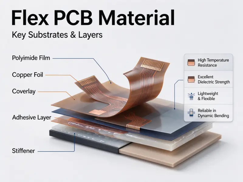
Material choice follows the environment and the frequency, not the price list. High-Tg FR-4 handles most digital boards, polyimide earns its place where temperature swings are severe, and low-loss laminates become necessary once the board carries RF or high-speed serial links.
A microvia is a copper barrel in a resin well, and the two expand at different rates. A laminate with a high coefficient of thermal expansion in the z-axis pushes more strain into that barrel on every cycle.
| Material family | Why programs choose it | What it costs elsewhere |
|---|---|---|
| High-Tg FR-4 | Availability, predictable processing, lower cost | Less margin at high temperature |
| Polyimide | Temperature capability, toughness | Moisture uptake, harder lamination |
| Hydrocarbon and PTFE laminates | Low loss for RF and radar | Weak dimensional stability |
Mixed builds are common on radar boards: low-loss material on the RF layers, FR-4 on the digital ones. For space hardware, outgassing is a separate screen, so material data sheets get checked against contamination limits before the stackup is locked.
Qualification, standards and documentation
Qualification is where an aerospace HDI program differs from a commercial one. The board has to be designed to IPC-2226, built to a declared performance class under IPC-6012, inspected against IPC-A-600, and backed by records that let the customer trace material, process and test results for the lot.
The documents that do the work:
- IPC-2226: design standard for HDI boards, including microvia construction and type designations.
- IPC-6012 Class 3 or 3A: the class high-reliability programs order to, with the space and military avionics addendum where the contract names it.
- IPC-A-600, IPC-9252 and IPC-4761: finished board acceptability, bare board electrical test, and via protection types.
- IPC-TM-650 2.6.26: interconnect stress test for plating and lamination quality.
- AS9100, AS9102 and AS5553: quality management, first article inspection and counterfeit avoidance.
Public research is worth reading before a design review. NASA’s Electronic Parts and Packaging program has published work on microvia reliability in high-density boards that ran HDI test vehicles through thermal cycling from −55°C to 100°C and 125°C. The failure analysis there is a reminder of how late these defects can appear.
The reports to read before you accept a lot
Ask for the coupon cross-sections, not just the pass stamp. Barrel copper thickness, fill quality, land alignment and lamination integrity all show up there. Ask whether inner layers got AOI before lamination, because a defect bonded into the stack cannot be reworked. On a Class 3 lot, also ask for impedance coverage, the microsection sampling plan, and whether first article inspection followed AS9102.
What drives HDI PCB price and lead time
HDI pricing follows process steps, not board area. Layer count, build-up cycles, microvia count and diameter, via fill, material family and test coverage set the price far more than panel size does. That is why PCB price comparisons between quotes often measure the wrong thing.
| Cost driver | Effect on price and lead time | Where the buyer has room |
|---|---|---|
| Layer count and build-up cycles | Each cycle adds drill, plate and press steps | Right-size the HDI type to the escape |
| Microvia diameter and aspect ratio | Tighter ratios narrow the process window | Stay inside the proven window |
| Via-in-pad fill and cap | Adds fill, planarization and inspection | Reserve it for fine-pitch BGA pads |
| Material family | Polyimide and low-loss cost more than FR-4 | Keep low-loss material where needed |
| Test coverage | Coupons and stress testing add days | Agree the sampling plan at quoting |
| Volume and panel utilization | Small lots and awkward layouts raise unit cost | Combine parts on a panel where allowed |
Two quotes can carry identical drawings and still describe different products. A board priced without microsection data and impedance verification is not the same item, and the gap tends to surface later as rework or a failed incoming inspection.
Specifying an HDI board for a defense build
A clean RFQ carries the stackup, the via map, the performance class, the material callout, the finish and the test plan. Anything left to interpretation gets decided by the fabricator, and that decision may not be the one the program needed.
- Fabrication data in a format the fabricator confirms it accepts, with drill files separated by via type.
- A stackup drawing with dielectric thicknesses, copper weights and impedance targets.
- A via map covering every microvia, blind via, buried via and via-in-pad location.
- The IPC-6012 class, the addendum if the contract names one, and a material spec with approved equivalents.
- Test and documentation: certificate of conformance, traceability, first article inspection.
DFM review belongs before the stackup is locked, not after the first lot fails. Once layer count and build-up structure are fixed, most of the cost and a good share of the risk are fixed with them. Ask about prototype-to-production continuity too: if the prototype ran on a different process, the validation data does not predict production behavior.
FAQ
Can an aerospace HDI board use FR-4?
Yes, and many do. High-Tg FR-4 is the baseline for digital boards in avionics and ground systems. The limits show up at high continuous temperature, in severe cycling, and above a few gigahertz, where a low-loss laminate becomes necessary.
How do you inspect microvias you cannot see?
With cross-sections, X-rays, and stress testing, roughly in that order of usefulness. Microsections show barrel thickness, fill quality, and land alignment on a sample basis. X-ray finds voids and misregistration without destroying the board. Interconnect stress testing puts a sample through repeated thermal excursions and measures resistance change, the closest thing to a direct read on plating.
Does HDI change assembly and rework?
It changes both. Filled and capped via-in-pad keeps the pad flat, so paste deposition and reflow behave normally, but rework can no longer wick solder into the via as a heat path. Thermal profiles have to account for a thinner board with more copper per unit area, and rework under a heat-sensitive fine-pitch part needs a preheat plan, not a hot air pencil.