Component pitches shrink; board outlines do not. A 0.4 mm pitch BGA with 300-plus balls leaves no legal space for a dog-bone fanout, and a layout that routed cleanly at 0.8 mm has nowhere to go. It stops being a routing exercise and becomes a process decision. Most quotes an HDI PCB manufacturer returns come down to three choices made before the first trace: how many build-up layers the escape needs, how deep the microvias go, and whether the simplest via structure that works was picked.
HDI PCB design is the practice of planning a board around laser-drilled microvias and sequential lamination instead of through-hole vias, so fine-pitch parts can escape in a smaller outline. The work sits in the stackup, not the schematic: choose the build-up structure, define every via span, size the pads to the drill, then route. Done in that order, a dense board is ordinary to build. Done in reverse, it is expensive or unbuildable.
The sections below follow that order, from stackup to the file package a fabricator receives.

What makes a PCB design HDI
A design is HDI when it needs microvias and sequential lamination to route, not when it merely looks crowded. The usual thresholds are traces and spaces at or below 100 µm, vias at or below 150 µm, pads around 400 µm or smaller, and a capture pad density above 20 per square centimeter.
The HDI PCB meaning blurs because the label gets applied to anything with small features. The distinction is structural. A conventional board is drilled once, after lamination, and every via crosses every layer in its path. An HDI board is built in stages: laminate the core, drill, add dielectric and copper, laser-drill, fill, repeat on the other face. Two boards can carry the same netlist on different process routes, which is why pcb board design for dense assemblies starts at the stackup.
| Design feature | Conventional multilayer | HDI build-up |
|---|---|---|
| Via formation | Mechanical drill after lamination | Laser microvia per build-up layer |
| Via diameter | 0.2 to 0.3 mm | 75 to 150 µm |
| Line and space | 100 µm and up | 75/75 µm common |
| Layer changes | Through vias block inner channels | Microvias free the layers beneath |
| Main cost driver | Layer count | Sequential lamination cycles |
Those ranges follow IPC-2226 and published capability tables, not your supplier’s actual numbers.
What pushes a board into HDI territory
- A fine-pitch BGA or chip-scale package that cannot escape with drilled vias.
- A pin count high enough that escape routing eats more channels than the inner layers offer.
- An outline fixed by the enclosure, so layer count cannot buy area.
There is also a case for skipping HDI. If the finest pitch is 0.65 mm or coarser, conventional pcb manufacturing with 0.15 mm traces usually routes the netlist for less. HDI on a design that does not need it buys cost without density, a recurring problem in consumer pcb electronics programs where the package is fixed early.
Read the stackup notation before you fix a layer count
The notation says how many build-up layers sit on each face of the core, nothing more. 1+N+1 has one sequential lamination per side, 2+N+2 has two. Materials, copper weights, via spans, and finished thickness sit outside that label.
Write the stackup as a table, not a label: copper layer, weight, dielectric above and below, via spans, lamination stage. Two engineers can agree on 1+N+1 and picture different boards, and the gap shows up when the fabricator asks which layer pairs connect.
What each build-up label commits you to
| Structure | Copper layers added | Typical use | Process reality |
|---|---|---|---|
| 1+N+1 | Two, one per face | Moderate-density BGA | Fewest steps, lowest risk |
| 2+N+2 | Four | 0.5 mm pitch BGA | Two steps per face |
| 3+N+3 | Six | Dense processors | Three steps, more drift |
| ELIC or any-layer | Varies | Extreme package density | Every layer pair drilled and filled |
Eight layers can be 1+6+1 with a six-layer core, or 2+4+2 with a four-layer core. Same count, not interchangeable. The second costs more, needs tighter registration, and offers escape paths the first cannot. Every transition a signal can make belongs in the span table before release.
Microvia rules that decide whether the board can be built
The binding constraint is aspect ratio, the drilled depth divided by the drilled diameter. Keep it at or below 1:1 and aim for 0.75:1. A microvia too deep for its diameter plates unevenly, and no inspection downstream recovers a void inside a 100 µm hole.
The arithmetic runs while you pick dielectrics. A 75 µm dielectric with a 100 µm target gives 0.75:1. Drill the same dielectric at 60 µm and you get 1.25:1, outside what most shops plate with confidence. Diameter follows thickness.
Capture pads follow the same logic. A pad about 100 µm larger than the via leaves ring for registration drift, with 50 µm a common floor. Squeezing the pad for routing space is a fast route out of the process window.
Three standards govern this layer. IPC-2226A, the 2017 revision of the sectional design standard for HDI printed boards, defines construction types and feature sizes. IPC-6016 covers HDI layer qualification, and IPC-6012 covers finished board acceptance. A Type III board is not automatically Class 3.
Stacked, staggered and skip vias
| Structure | How it connects | Fill | Reliability exposure |
|---|---|---|---|
| Staggered | Offset between layers | Not required | Lowest |
| Stacked | Piled on each other | Required | Higher, aligned interfaces |
| Skip | Bypasses one layer | Varies | Moderate, span must be explicit |
| Buried | Inner core layers | Core dependent | Fixed at lamination |
Staggered is the safer default and costs less: the microvias do not share a vertical axis, so plating interfaces spread out. Stacked microvias solve vertical escape when no lateral room is left, and only work when the lower via is filled and planarized before the next lamination. Stacking on a buried core hole is the combination most likely to fail thermal cycling. This is where hdi pcb fabrication realities arrive early, since every stacked level adds a registration risk and a fill step.
BGA escape and via-in-pad
Escape follows pitch, not preference. Down to about 0.8 mm, dog-bone fanout with drilled vias works. At 0.65 mm and below, microvias take over. At 0.5 mm and finer the via sits inside the pad, because no gap between pads is wide enough.
| BGA pitch | Fanout method | Via type | Build-up needed |
|---|---|---|---|
| 0.8 mm | Dog-bone | Through or microvia | Optional |
| 0.65 mm | Dog-bone with microvia | Laser microvia | 1+N+1 |
| 0.5 mm | Via-in-pad | Filled microvia | 1+N+1 or 2+N+2 |
| 0.4 mm and finer | Via-in-pad, stacked | Filled microvia | 2+N+2 or ELIC |
Via-in-pad is a finished process, not a placement decision. Drill, plate, fill with epoxy or copper, cure, planarize, cap plate, until the pad is flat enough for paste. A dimple under 25 µm is the usual limit, and many assemblers want under 15 µm on fine-pitch pads. Skip planarization and the result is solder wicking into the barrel, or a joint that passes X-ray and fails thermal cycling.
Route outside in. Outer rows have room and escape first; inner rows take via-in-pad. One method across the array beats mixing.
Signal integrity rules that still apply on a dense board
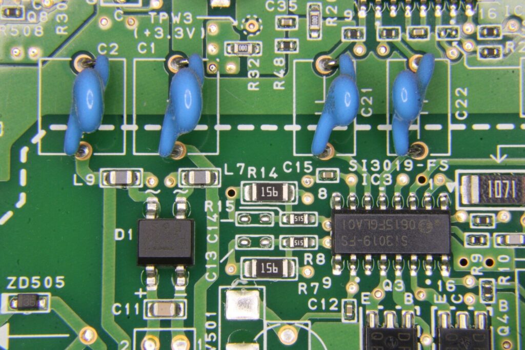
Density compresses routing space; it does not relax return current. Every high-speed trace still needs a continuous plane beneath it, and every layer change needs a ground via nearby to carry the return path across. A dense board with split planes performs worse than a larger one without them.
The electrical gain from HDI is real but narrow. A microvia ends on its target layer, so no stub remains, and stub reflection is what limits a through via above a few gigahertz. The gain disappears if the microvia lands on a slotted plane. For a pcb circuit running multi-gigabit links, plane continuity beats via technology, and a high-speed PCB stackup with disciplined planes will beat a denser one without them.
Controlled impedance is the other half. Thin build-up dielectrics mean narrow 50 Ω lines and a harder impedance hit from thickness error. Put the target and tolerance on the drawing, and ask for a coupon on the real routing layer.
What the 3H rule means in an HDI layout
The 3H rule sets center-to-center spacing between adjacent parallel traces at no less than three times the dielectric height H, measured to the nearest reference plane. With 4 mil of dielectric under the trace, neighbours sit at least 12 mil apart.
The target is crosstalk. A thin dielectric pulls field lines close to trace and plane, so the same spacing couples less; a thick one spreads them, so the gap grows. 3H handles the electric field and pairs with 3W for the magnetic side.
On an HDI board the rule holds everywhere except where it cannot. In a BGA escape region 3H spacing is often impossible, so shorten the parallel run, keep a plane underneath, put aggressor and victim nets on separate layers, and check it in simulation. The same logic sets copper pullback at the board edge.
Material and copper choices that follow from the design
Lock the laminate before the stackup is frozen. Swapping material after prototype validation shifts Dk, changes the width needed for the same impedance, and can invalidate the laser recipe qualified for the original dielectric.
| Parameter | Why it matters | Working target |
|---|---|---|
| Tg | Deformation through lamination and reflow | 170°C or higher |
| Td | Stability in lead-free reflow | 320°C or higher |
| Dk | Impedance and propagation delay | 3.0 to 3.8 |
| Df | Insertion loss on long channels | Below 0.005 at 1 GHz |
| Z-axis CTE | Barrel and joint stress | Below 50 ppm/°C |
| Copper foil | Fine-line etching, loss | 9 to 12 µm fine lines, 35 µm power |
Thin copper and dielectric make 75 µm lines possible, and make the board fragile in process. A laminate that etches well at 12 µm copper will not carry a heavy power plane, so hdi boards mix weights by layer.
Where HDI PCB price actually comes from
Price tracks lamination cycles, panel area, fill-and-cap operations, and quantity far more than layer count. Two eight-layer boards can land at very different points on hdi pcb price because one needs one build-up step per face and the other needs two.
| Cost driver | What it adds | What you control |
|---|---|---|
| Lamination cycles | Drilling, plating, imaging, registration | Fewer layers where escape allows |
| Panel area | Material and utilization | Outline and panelization |
| Via fill and cap | Fill, cure, planarize, cap plate | Via-in-pad only on inner BGA rows |
| Layer count | Copper and dielectric per layer | Consolidating signal layers |
| Quantity | Setup amortization | Combining revisions into one order |
That is why a pcb price comparison on the same Gerber set returns unrelated numbers. One quote assumes two cycles, another four; one priced via-in-pad fill, the other treated it as drilling. Send the stackup and via span table with the files, and ask an HDI PCB board manufacturer for a production stackup before quoting. A quote built on an assumed stackup is not one.
Design review checklist before you release files
Run one structured review before the files leave your desk. Most HDI re-spins trace back to a stackup nobody checked for symmetry, a via span nobody defined, or a via-in-pad with no fill instruction.
- Confirm the construction type and build-up count against the real BGA escape, not a familiar template.
- Check symmetry: copper weight and dielectric balanced around the center, build-up layers matched on both faces.
- List every via span on the HDI board PCB drawing, microvia, buried, and through.
- Mark which microvias need fill and cap, and state the via-in-pad dimple limit.
- Check aspect ratio against the dielectric thickness actually specified, layer by layer.
- Put impedance targets, tolerances, and coupon locations on real layers, and confirm the hdi pcb manufacturing process matches the drawing.
- Name the acceptance standard and class, and state whether thermal stress or microsection is required.
Surviving this list does not guarantee a manufacturable board, but it removes the failures that come from documentation rather than engineering.
FAQ
Does HDI PCB design need a different CAD tool?
No, but it needs one that defines layer pairs and via spans explicitly. The stack-up editor has to carry dielectric thickness per layer, and the drill output has to separate laser from mechanical holes. Most of the pcb learning curve here sits in stackup literacy, not software.
Can rigid-flex or ceramic HDI boards reuse the same design rules?
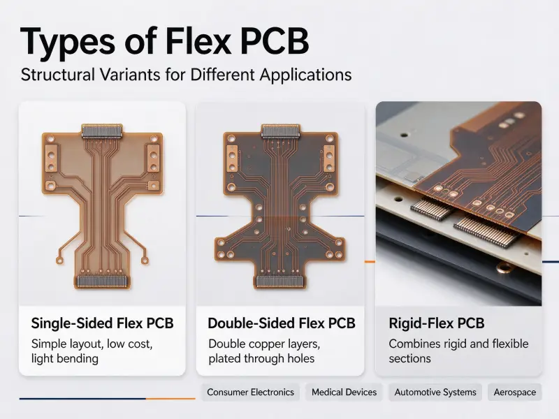
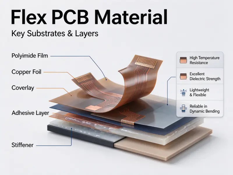
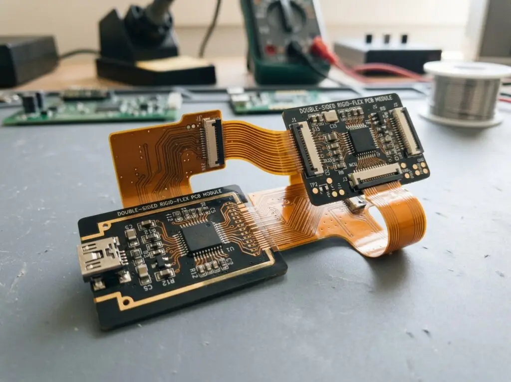
Only partly. Rigid-flex adds coverlay, bend radius, and flex-core lamination constraints on where microvias can sit, and ceramic substrates form vias differently. The aspect ratio logic holds, but material limits need re-qualifying.
Is a continuity test enough to prove microvia reliability?
No. Room-temperature continuity passes boards with plating that is thin but intact, and microvia failures show up after thermal cycling rather than at final test. Thermal cycling, interconnect stress testing, or microsectioning on a coupon exposes barrel cracks a netlist test cannot see.