A board that passed as advanced in 2021 reads as ordinary now. Phone mainboards route BGAs at 0.4 mm pitch, radar modules pack the same density into less space, and neither leaves room for a drilled via between pads. The build changes underneath: laser microvias, sequential lamination, and copper-filled via-in-pad. So does the quote. Buyers now ask whether one supplier can carry HDI PCB manufacturing and assembly through a single process.
An HDI PCB assembly service takes a finished high-density board, mounts components on it, solders them to a controlled profile, and tests the result. It does not fabricate the board. Those are two processes with two sets of failure modes, and a quote that blurs the line blurs where responsibility sits.
The definition comes first, because the term gets used loosely.
What does HDI PCB mean?
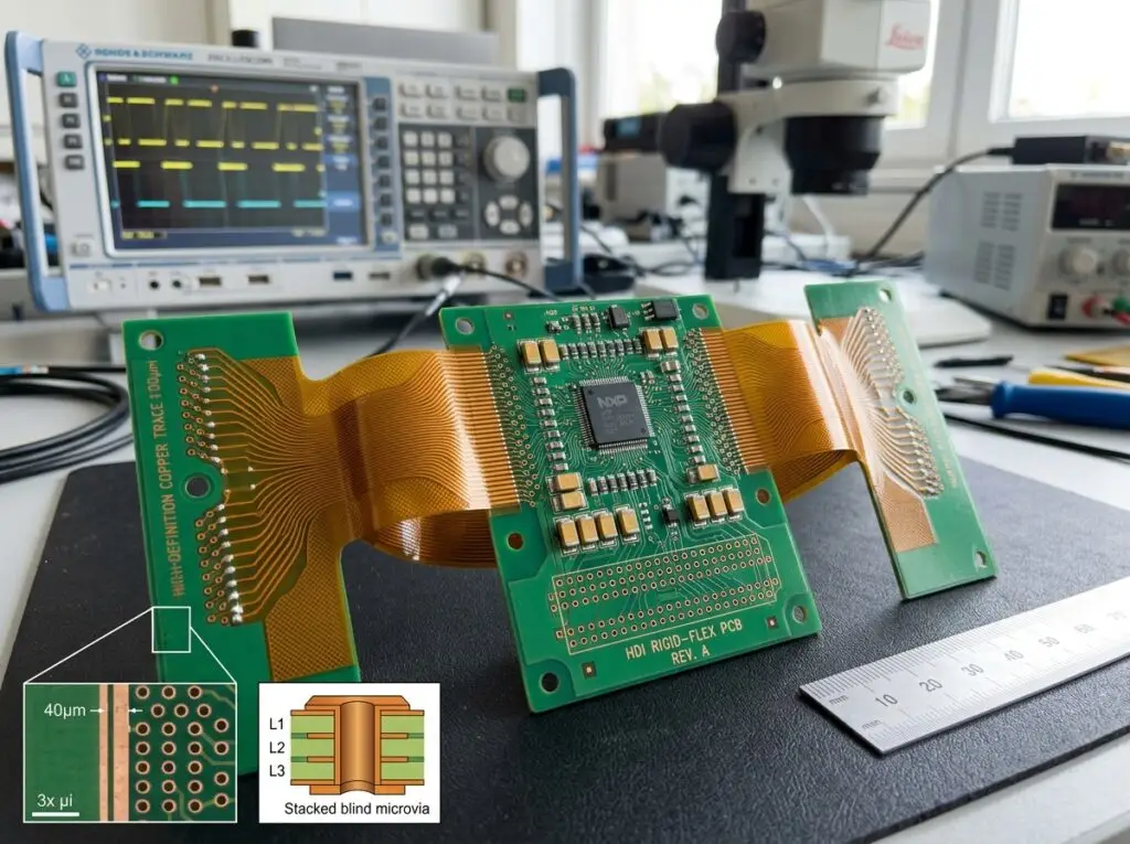
HDI describes how densely a board is built, not what it does. A board qualifies as high-density interconnect when its traces, vias and pads are fine enough that only laser drilling and build-up lamination can produce them.
The label is technical. A six-layer board with 0.2 mm through-holes is a conventional multilayer however many parts it carries, while an eight-layer board with laser microvias and 75 μm outer traces is HDI even with fewer components.
The geometry that separates HDI from a standard board
IPC-2226, the sectional design standard for high-density interconnect boards, sets the thresholds: line width and spacing at or below 100 μm, via diameter at or below 150 μm, capture pads below 400 μm. IPC-2226 is what shops cite when a design sits near the boundary.
Below those limits, mechanical drilling is the bottleneck. A bit rarely goes under 0.25 mm, every through-hole eats routing space on every layer it crosses, and hole depth sets an aspect ratio plating must cover evenly.
Microvias, blind vias, buried vias, and via-in-pad
- Microvias are laser-drilled, usually 0.05 mm to 0.15 mm across and under 0.25 mm deep. The low aspect ratio makes plating reliable.
- Blind vias reach an outer layer to one or more inner layers without crossing the board.
- Buried vias connect inner layers only and never reach the surface.
- Via-in-pad puts the microvia inside the component land, shortening the current loop to the power planes.
Via-in-pad is where fabrication and assembly collide. An unfilled via inside a pad wicks solder down the hole during reflow, and the joint starves. The fix belongs upstream: copper fill, planarisation, then plating over the pad.
How stack-ups get named
Engineers count microvia layers per side of the core; the standard counts structure types.
| Build-up | Microvia layers per side | Lamination cycles | Where it shows up |
|---|---|---|---|
| 1+N+1 | 1 | 1 | Industrial controllers, consumer boards with one fine-pitch device |
| 2+N+2 | 2 | 2 | Automotive modules, telecom line cards, denser fan-out |
| 3+N+3 | 3 | 3 | High pin-count processors, computing modules |
| Any-layer | Every layer pair | 4 or more | Phone mainboards, space-constrained modules |
IPC-2226 calls these Type I to Type VI, and each added layer pair means another lamination cycle and another chance to lose yield. Stack-up is a cost decision before it is a technical one.
Where fabrication ends and assembly begins
The handover point is bare-board electrical test. Everything before it belongs to the board shop, everything after it to the assembler, and defects created before the handover are usually invisible to the assembler’s inspection.
HDI PCB manufacturing splits into four steps that decide what arrives. Laser drilling sets via geometry, with UV or CO₂ chosen by material; glass reinforcement in FR-4 scatters the beam. Desmear cleans the via base, and incomplete removal traps gas that later shows as a void. Plating fills and levels the via, and the flatness of that fill sets how much paste the stencil can deposit. Sequential lamination bonds each pair, and registration drift pushes vias off target.
What the assembler inherits from the board shop
- Surface finish and shelf life. ENIG and OSP both solder well when fresh and both degrade in storage.
- Warpage. A thin stack that bows beyond the placement window misplaces parts at 0.4 mm pitch.
- Fill dimples. A shallow depression in a via-in-pad holds less paste than the stencil aperture assumes.
- Solder mask registration. On 75 μm traces, a shift of tens of microns changes how much copper the pad exposes.
- Voids at the via base. Invisible on AOI, harmless in functional test, and the first thing to crack after thermal cycling.
None of this can be inspected away downstream, so catch it at goods-in: fabrication drawing with stack-up and impedance targets, Gerber or ODB++ matching the revision, the bare-board test report, impedance coupons, microvia cross-sections with the coupon marked, and the surface finish date code.
What an HDI PCB assembly service actually does
It places components on the board, forms the joints, and answers for whether the assembly works. The work runs from DFM review to first-article approval, and the board itself comes from somewhere else.
From DFM review to first article
The DFM review is the cheapest hour of the project. Board design gets checked against the parts: land patterns against the part, via locations against the placement file, and the panel against its fit. Most of what goes wrong later announces itself here.
| Step | What it does | Failure it prevents |
|---|---|---|
| DFM and stack-up review | Checks land patterns, via placement, panel fit | Pads that cannot print, vias under a component |
| Stencil printing | Deposits paste by aperture area | Bridging at fine pitch, starved thermal pads |
| Placement | Positions parts to machine accuracy | Tombstoning, shifted QFNs, skewed connectors |
| Reflow under nitrogen | Forms the joint to a measured profile | Voids, cold joints, warped thin boards |
| First article | Confirms the build matches the drawing | Repeating the defect for a whole lot |
Nitrogen earns its cost on HDI. Thin dielectric and small pads leave little margin in the reflow window, and oxidation on a 0.4 mm pitch pad costs wetting.
What turnkey adds
A turnkey PCB assembly quote covers components as well as labour, which moves supply risk to the supplier. Worth paying for on a board with 800 placement positions and four single-source parts; not worth paying for on catalogue parts the buyer already stocks.
Consigned material works the other way: the buyer supplies the parts and carries the loss when a reel is bad. With turnkey the supplier buys, verifies and manages obsolescence, and the quote should say how substitutes get approved.
Most HDI assembly failures that reach the customer are not placement failures. They come from a BOM that does not match the board revision, or a stack-up change nobody told the assembly house about.
Design rules that decide whether the assembly yields
Four constraints decide most of the outcome: microvia aspect ratio, via-in-pad filling, fine-pitch escape routing, and the balance between impedance, copper distribution and thermal path.
Microvia aspect ratio and stacked versus staggered
A via twice as deep as it is wide is hard to fill and harder to plate evenly. Depth under 0.25 mm at 0.1 mm diameter keeps the ratio near 1:1.
Stacked microvias save board area and concentrate thermal stress in one column; each lower via must be filled before the next level is drilled. Staggered microvias spread the stress and survive more cycles, at the cost of routing space. Most builds stop at two or three stacked levels.
Fine-pitch BGA and escape routing
Below 0.4 mm ball pitch, a dog-bone fan-out stops fitting between the pads. The escape runs through via-in-pad or the design moves to a finer stack-up, and that decision sets the layer count, the lamination count and half the price.
Thermal and impedance constraints
Dense routing in a thin stack traps heat, so thermal via arrays under power devices need a path to a copper plane with enough copper left after routing to spread it. Controlled impedance needs known dielectric thickness, and symmetrical builds warp less, which is the part of HDI PCB design most often skipped.
How much does it cost to assemble a PCB?
Per-board price comes from five buckets: one-time engineering, the bare board, the bill of materials, placement and soldering, and test. Volume spreads the first bucket across more boards; the board’s density sets the rest.
NRE covers the stencil, programming and first article, charged once per build. The bare board scales with layer count, build-up and microvia count. The BOM depends on component mix and single-source parts. Assembly follows placement count, and test follows coverage.
How price moves with quantity
Published 2026 assembly pricing tables, checked 20 October 2026, put all-in per-board cost in these ranges, with setup amortised across the run. The figures are directional, not a rate card.
| Boards | Simple two-layer | Mid four-layer | Eight-layer and HDI |
|---|---|---|---|
| 5 | $20 to $80 | $60 to $120 | $150 and up |
| 25 | $12 to $40 | $45 to $90 | $120 to $200 |
| 50 | $10 to $35 | $40 to $80 | $100 to $180 |
| 100 | $8 to $25 | $35 to $70 | $90 to $160 |
| 250 | $6 to $20 | $30 to $60 | $80 to $150 |
| 500 | $5 to $15 | $25 to $55 | $70 to $130 |
| 1,000 | $4 to $12 | $20 to $45 | $60 to $120 |
The steepest drop sits between 5 and 100 boards, where NRE amortisation does the work. Past 250 the curve flattens. The HDI column runs higher at every tier, and its low-volume end is the least reliable number here, because first-build yield varies more than a table can show.
Why HDI carries a premium at low volume
Each layer pair adds a lamination cycle with its own registration and its own scrap. Laser drilling is slower per hole than mechanical drilling, and fill plus planarisation add plating hours. Then yield does the rest: a mature conventional board reaches a yield a first HDI build will not.
Ask for the split, not the total. An itemised quote lets two suppliers be compared on the same basis, and shows which line is out of step when an HDI PCB price comes back high.
Which tests prove an HDI assembly is good
AOI proves placement and visible joints. X-ray proves hidden joints and via fill. Cross-section proves the microvia structure. In-circuit and functional test prove the board works. None of them covers the others.
| Method | Proves | Cannot see |
|---|---|---|
| AOI | Placement accuracy, fillet shape, missing parts | Anything under a BGA or shield can |
| X-ray | Hidden joints, void percentage, via fill height | Plating thickness at the via base |
| Cross-section | Microvia barrel, fill, alignment between layers | The rest of the panel |
| Flying probe or ICT | Opens, shorts, component values | Timing margins and function |
| Functional test | The assembly works as designed | A marginal joint that fails in the field |
Acceptance criteria come from the IPC workmanship and performance standards, and the class matters. Class 3 allows less voiding and tighter tolerance than Class 2, and the difference shows up in inspection time and scrap, not materials.
“100% AOI” is not a quality claim on its own, because every BGA is invisible to it. What matters is whether X-ray coverage is full or sampled, whether cross-sections come per panel or per lot, and who signs the report.
How to qualify an HDI PCB assembly supplier
Four things separate suppliers that can hold an HDI build from those that broker it: whether fabrication is in-house, what their microvia fill and cross-section data look like, how much of the board they test, and how change and traceability are handled.
Worth asking before a first order: is HDI fabrication in-house, and who owns the stack-up review? How is via-in-pad filled and planarised? Is X-ray coverage full or sampled? Can the line rework a 0.4 mm pitch BGA, and what is the limit per board? How are changes notified, and which revision is quoted? Will the quote be itemised?
Then run the build in three steps: approve the first article against the drawing rather than a photo, pull a cross-section from a different panel, and put a sample through thermal cycling before committing the annual volume.
FAQ
Can an HDI board survive a second reflow or a rework cycle?
Usually, within limits. The risk sits in the microvia stack, not the solder joint. Each reflow adds thermal stress to filled vias, and a stacked structure accumulates it in one column. Builds with two or three stacked levels handle a second pass in most cases; any-layer builds have less margin.
Does HDI change minimum order quantity and lead time?
Both, and not because of tooling. MOQ is driven by panel utilisation, since an HDI panel carries fewer boards than a conventional one of the same size. Lead time grows at lamination, where each build-up cycle adds a queue step, and at first article.
Is 1+N+1 enough for a fine-pitch BGA, or do I need 2+N+2?
It depends on how many signals have to escape and where they go. A single fine-pitch device with a short escape fits on 1+N+1. Two dense devices whose routes cross, or routing between ball pads on both sides of the core, pushes the design to 2+N+2. Let the routing study pick the stack-up.