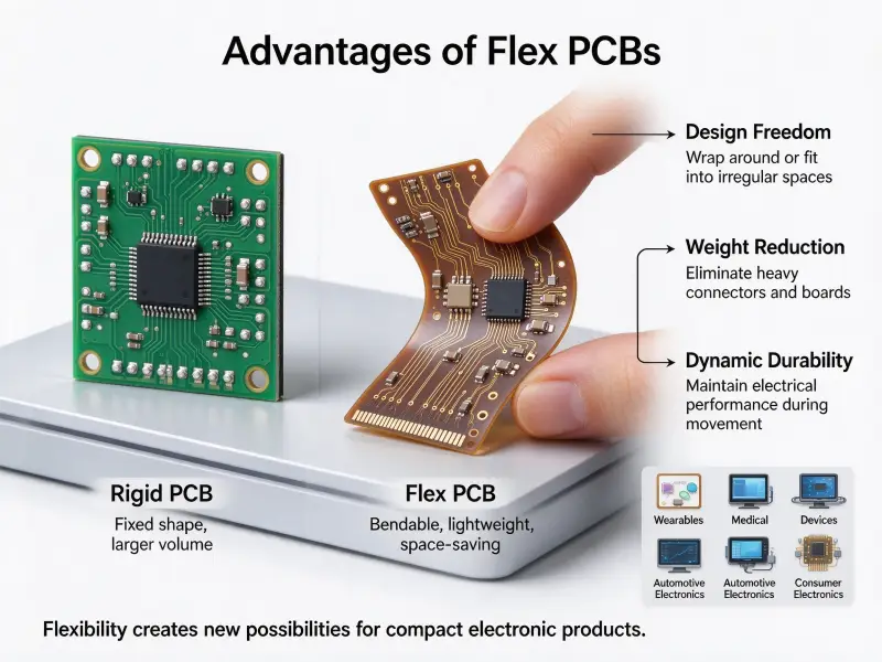
There’s a moment in most compact hardware projects when the board has to fold. A display sits at an angle to the main logic, a sensor has to reach past a hinge, or the housing curves and a flat laminate simply will not follow it. At that point the question stops being “which board” and becomes “how do I actually make one of these.”
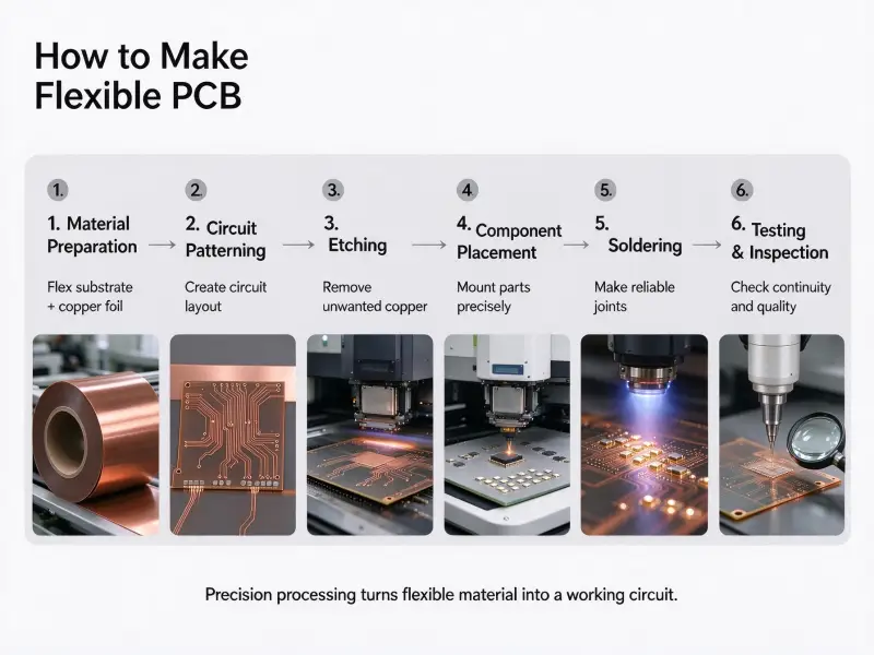
Making a flexible PCB is three separate jobs, not one. You need design data a fabricator can read, a build stage that puts copper on polyimide without cracking it, and an assembly stage that mounts parts on a surface that bends. Which route you take, a bench build, a prototype run or a volume order, is set by your layer count, whether you need plated holes, and whether anyone has to place components on the finished circuit.
The routes overlap less than most guides suggest, so it is worth seeing them side by side before choosing a flexible PCB supplier or buying film.
Three routes, and what each one can actually produce
A flexible PCB can be made at a bench, at a quick-turn prototype shop, or on a production line. The bench route gives you one copper layer, no plated holes and a taped-on cover layer. The prototype route gives you real plated vias, pressed coverlay and a cut profile. The volume route adds tooling, panelization, test fixtures and yield control.
| Bench build | Quick-turn prototype | Volume production | |
|---|---|---|---|
| Layers | 1 | 1 to 6 | 1 to 10, higher on request |
| Plated holes | No, eyelets or bridges | Yes | Yes, including microvias |
| Cover layer | Kapton tape or liquid PI | Pressed coverlay film | Pressed coverlay, or photoimageable mask |
| Profile | Scissors or knife | Laser or die cut | Laser, die or rout, panelized |
| Component assembly | Hand solder only | Stencil, reflow, carriers | Full SMT line with fixtures |
| Cost per part | Lowest at quantity one, highest per feature | Middle | Lowest per unit, highest upfront tooling |
| Lead time | Hours | Days | Weeks, plus tooling |
The cost column is where the routes get misread. A bench build wins on a single board because there is no tooling, and loses the moment you need a second layer. Prototype pricing is not production pricing, and a [flexible PCB price] comparison only makes sense at the same layer count, same finish and same test requirement.
When the bench route stops paying off
The bench route is honest about its limits, and they arrive quickly.
- No plated through holes. A via between two copper layers needs electroless seeding and electrolytic build-up. A soldered wire through a hole is not the same thing, and it will not survive bending.
- Cover layer adhesion. Hand-applied tape traps air. Air pockets lift during reflow and take traces with them.
- Registration. Pad openings in a hand-cut cover layer drift by tenths of a millimetre. That is fine on a 2 mm pitch header and useless on a 0.5 mm connector.
- No controlled impedance. Without a defined stack-up and a known dielectric constant, you cannot hold a target on any high-speed net.
If your design has two layers, a fine-pitch connector or an impedance requirement, the bench route has already ended.
Design rules that decide whether the board can be built
Most boards that “cannot be made” are not impossible. The drawing is missing the information that decides how they get built: which zones bend, how far, how often, where the stiffeners sit, and how thick the finished part should be. Fix the drawing and the same design becomes routine.
Static fold or continuous flexing
These are two different products that share a material. A board that folds once during assembly can be creased tightly and never thought about again. A board that flexes in service is a fatigue part, and the copper, the thickness and the radius rules all change.
The IPC-2223 sectional design standard, listed among the IPC design standards, separates flexible boards by installation use, covering whether the part bends during installation only or keeps moving afterwards. Fabricators read that classification before they quote, because a dynamic part changes the material call, the copper type and the bend radius they will accept. State the class, the inside radius and the expected cycle count on the drawing rather than leaving them to be guessed.
For dynamic work, rolled annealed copper is the usual call, since its grain runs along the rolling direction and takes repeated bending better than electrodeposited foil. For a one-time fold, electrodeposited copper is cheaper and adequate. This is the single decision in flexible pcb design most often made by default rather than on purpose.
Stack-up and flexible pcb thickness
Finished thickness is the sum of what you laminate, and every layer you add buys routing space at the cost of bend radius. A single-sided build lands around 0.1 mm; the same circuit with a second copper layer, an adhesive system and a thicker coverlay can pass 0.3 mm without any component on it.
| What you add | Typical value | What it does to the bend |
|---|---|---|
| Base film | 25 µm polyimide | Sets the floor; thinner film bends tighter |
| Adhesive layer | 20 µm | Adds thickness and a lower-temperature layer that can fail first |
| Copper | 18 µm or 35 µm | 35 µm is 2 oz territory and belongs out of bend zones |
| Coverlay plus its adhesive | 25 µm plus 20 µm | Protects traces, stiffens the bend |
| Stiffener | 0.2 mm to 1.0 mm locally | Removes bendability where it sits, by design |
Two rules follow. Keep the bend zone free of anything you do not need there, and put your thickness target on the drawing as a tolerance, not a wish. A flexible pcb thickness range of 0.05 mm to 0.5 mm covers most standard work, but the number that matters is your number.
Routing through a bend zone
Traces in a bend behave like a metal hinge. They survive when they run along the axis of the bend and fail when they cross it at a right angle.
- Run conductors parallel to the bend line, never perpendicular to it.
- Keep vias out of the bend zone entirely. A plated barrel is a stress riser with no give.
- Avoid solid copper pours across the bend. Use hatched or cross-hatched fill if you need shielding.
- Taper trace entries with teardrops at pads, so a crack has nowhere to start.
- Stagger conductor widths rather than running a bundle of identical traces, which concentrates stress on the same line.
- Stay out of the bend with heavy copper and with any component, including zero-ohm links.
Stiffeners and flexible pcb connector tails
A flexible pcb connector needs a rigid landing area. Insertion force goes straight into the film, and without support the pads smear or delaminate. A polyimide stiffener of 0.2 mm or 0.3 mm under the tail is the usual answer, chosen so the finished tail matches the connector’s specified thickness, commonly 0.2 mm or 0.3 mm for a zero insertion force style.
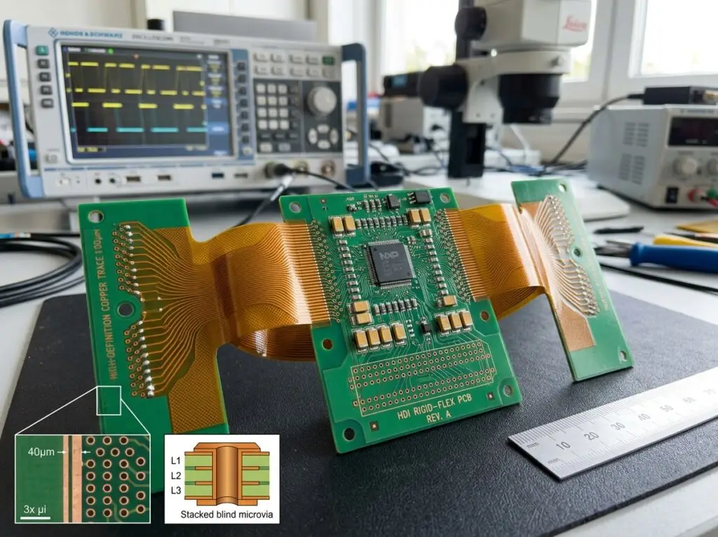
Stiffeners are also the cheap alternative to a rigid-flex build. Where a design needs a few rigid islands and one or two bending sections, a plain flex board with FR4 or steel stiffeners often does the job for less money. Where the rigid areas carry dense circuitry or many components, a rigid-flex PCB manufacturer build is the cleaner answer, and it removes the connectors between sections altogether.
Making one at the bench, step by step
A one-off flexible board is buildable at home in an afternoon if you accept one copper layer, no plated vias and fat features. You need copper-clad polyimide film, a way to put a resist pattern on it, an etchant, and something to cover the traces afterwards.
- Design the circuit with generous traces, at least 0.2 mm wide, no acute angles, and a stiffener island drawn where anything mounts.
- Buy copper-clad polyimide, single-sided, in a thickness you can still cut with scissors.
- Print the pattern as a mirror image, either as toner onto transfer paper or onto transparency film for a dry-film resist.
- Transfer it. Toner goes on with heat and pressure from a laminator or an iron; dry film needs UV exposure and development.
- Etch in ferric chloride or ammonium persulfate, agitating, and pull the board the moment the unpatterned copper clears. Polyimide is more forgiving than FR4 here only because there is so little copper to remove.
- Strip the resist with acetone and inspect under magnification before you go further.
- Cover the traces with polyimide tape, or spin or brush a thin liquid polyimide and cure it. Leave pad windows open.
- Bridge any layer change with an eyelet, a wire link or a zero-ohm resistor, then test continuity before soldering.
What a home build gives up
You lose plated holes, coverlay registration, controlled impedance, a real solder mask and a clean cut edge. What you keep is the part that matters early: you find out whether the shape folds the way you drew it, whether the traces fit through the hinge, and whether the connector lands where the housing expects. That is worth an afternoon, and it is not a path to a production part.
What a prototype build adds
A prototype shop replaces every hand step with a process step: dry film imaging instead of toner, laser drilling instead of a hand drill, plated barrels instead of wire links, and a vacuum press instead of tape. The result is a board that behaves like the production part, because it was built the same way.
The difference that shows up first is registration. Coverlay openings are cut or laser drilled from the same data as the pads, then bonded under heat and pressure in a vacuum press, so an opening lands where it was drawn. The difference that shows up in testing is that every circuit gets a flying probe check with soft contacts, which will not dent a pad on a 0.1 mm thick part.
Prototype and volume builds diverge at tooling, not at precision. A prototype panel is laid out for speed. A production panel is laid out for parts per sheet, and the outline you drew may get adjusted to improve utilization, which is a conversation worth having before tooling is cut. Ask what the panel looks like, not just what the board looks like.
Assembling components onto a flex circuit
Flex assembly is not rigid assembly on thinner material. The board has no stiffness of its own, so it needs a carrier or a pallet, and it absorbs heat differently, so the reflow profile changes. Boards that pass fabrication and fail in the field usually failed here.
- Support the board. Double-sided tape on a carrier, or a dedicated pallet, holds the circuit flat through printing and placement. Unsupported film sags under stencil pressure and smears paste.
- Bake before reflow. Polyimide absorbs moisture. A pre-bake prevents the blistering that appears as a lifted coverlay after the first pass through the oven.
- Back the connector area. A stiffener under the tail, or a support block under the part during placement, keeps insertion force off the film.
- Skip through-hole clinching. Bending leads over on a flexible board cracks the pad. Use selective soldering or move to a surface mount part.
- Underfill or glob top. Anything that sees vibration or repeated flexing benefits from local reinforcement around the joint, not across the bend.
- Handle without creasing. A crease is a permanent crack starter. Parts travel flat, in trays, never folded into a bag.
Checking the first article
Five checks catch nearly everything: continuity and isolation, a microsection of the plated holes, dimensional and coverlay registration, a bend test at the declared radius, and adhesion at the stiffener and connector tail.
Continuity and isolation confirm the pcb circuit matches the netlist. A microsection shows whether the plating is thick enough and ductile, which is where a cracked barrel starts. Registration is measured against the drawing, not by eye. Bend testing to the cycle count you declared is the only way to know a dynamic design will survive, and it should be run on parts from the same panel as production. Adhesion pulls at the two places where a flex board separates: stiffener edges and coverlay corners.
Where builds fail, and which stage is to blame
A failure symptom usually points at one stage. Reading it backwards saves time, because the fix is rarely where the failure appears.
| What you see | Likely stage | What to change |
|---|---|---|
| Coverlay lifting after reflow | Assembly or lamination | Bake before reflow, check press cycle and adhesive lot |
| Cracked traces at the bend | Design | Reroute along the axis, add teardrops, thin the stack-up there |
| Open via after bending | Fabrication or design | Ductility of the plating, and keep vias out of the bend |
| Pads lifted at the connector | Assembly | Stiffener thickness, insertion support, lower soldering temperature |
| Etched trace narrower than drawn | Fabrication | Etch compensation in CAM, tighter line width control |
| Delamination between film and copper | Material or lamination | Adhesiveless construction, moisture control before press |
None of these are mysterious once the stage is named. What makes them expensive is discovering them at volume, which is why the first article deserves the bend test and the microsection rather than a visual pass.
FAQ
How long does it take to make a flexible PCB?
It depends on the route. A bench build is an afternoon. A prototype order typically moves through fabrication in days, with the schedule set by drilling, plating and coverlay pressing rather than by the layout. Volume builds run weeks, and the clock starts at tooling and material release, not at the purchase order. Add extra time for a first article you intend to bend test, because that test needs parts off the production panel.
What is the smallest quantity I can order?
Prototype quantities as low as one piece are normal for flexible boards, and per-part cost at that volume is dominated by setup rather than material. Volume pricing starts where panel utilization and tooling amortization begin to work, which is a function of part size and layer count more than an arbitrary number. Ask what the setup charge covers before comparing two quotes.
What is the difference between a flexible PCB and a flat flexible cable?
A flat flexible cable is a conductor run with a fixed pattern and no components. A flexible PCB carries etched circuitry, can have multiple layers, plated vias and mounted parts, and is designed against a bend radius and cycle count. The two overlap in appearance and are not interchangeable: a cable has no place to put a decoupling capacitor, and a circuit has features a cable house will not quote.