High-Frequency PCB Manufacturing for 5G Small Cell RF Front-Ends
Sub-6 GHz Optimized | RO4350B + IT-180A 8-Layer Hybrid | ±1.8° Phase Match
- Insertion Loss < 0.15 dB/inch @ 3.5 GHz
- Dk 3.48 ± 0.05 - Tight Dielectric Tolerance
- VLP Copper + Plasma Pre-Treatment
Request a Quick Quote
ISO 9001:2015
Certified Quality Control
Rogers RO4350B
100% Genuine Laminate
IPC-6012 Class 3
Telecom-Grade Standard
RoHS & CE
Fully Compliant
100% VNA E-Testing
S11 & S21 Verified
High-Frequency PCB Types by Stackup & Structure

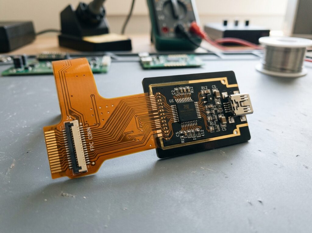
Double-Sided RO4350B PCB
The baseline high-frequency build: two RO4350B-clad copper layers laminated into a single low-loss substrate, routed with controlled 50 Ω impedance from the connector launch to the antenna port. No hybrid transition, no extra interfaces – the cleanest path for a short RF chain.
- Ideal for Sub-6 GHz antenna feeds, filters and simple RF front-end chains
- Dk 3.48 ± 0.05 keeps propagation delay repeatable lot to lot
- Lowest-cost route into genuine Rogers-grade RF performance at low layer counts
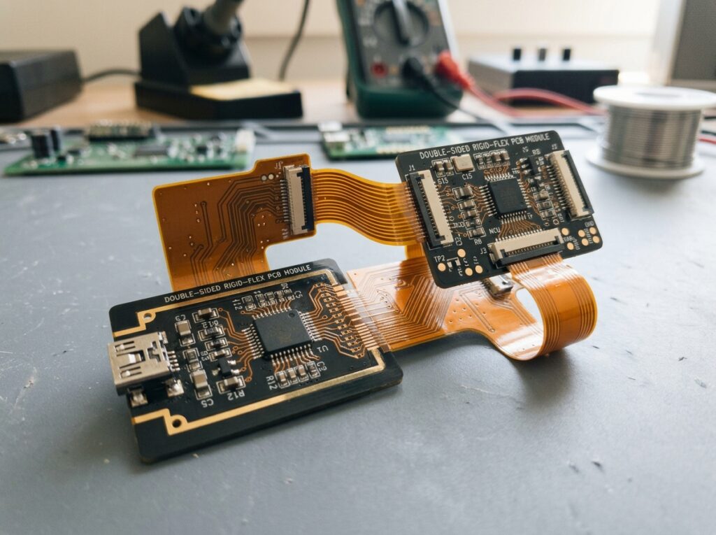
8-Layer RO4350B + IT-180A Hybrid
The workhorse 5G small cell stackup: RO4350B on the outer RF layers for low-loss transmission lines, IT-180A high-Tg FR-4 cores and prepregs for power, ground and control layers, laminated into one 1.6 mm hybrid board with RO4450F bondply at the RF interface.
- Premium RF laminate only where RF actually propagates – material cost cut by 30-40%
- RO4450F bondply at the RF / FR-4 interface keeps Dk stable through the lamination cycle
- Suitable for massive MIMO arrays, RRU boards and 5G small cell radio units
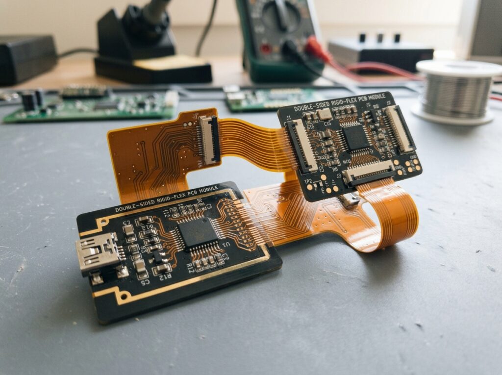
Multi-Layer PTFE PCB
For millimetre-wave and very high frequency designs, pure PTFE or hydrocarbon laminates (Rogers RT5880, Taconic TLX) deliver the lowest dissipation factor available. Multi-layer PTFE builds need specialised plated-through-hole conditioning and tightly controlled lamination cycles.
- Df as low as 0.0009 for the lowest insertion loss at Ku-band and above
- Plasma plus sodium-etch PTH treatment prevents wicking and barrel cracking
- Used for radar, SATCOM and phased-array antenna modules
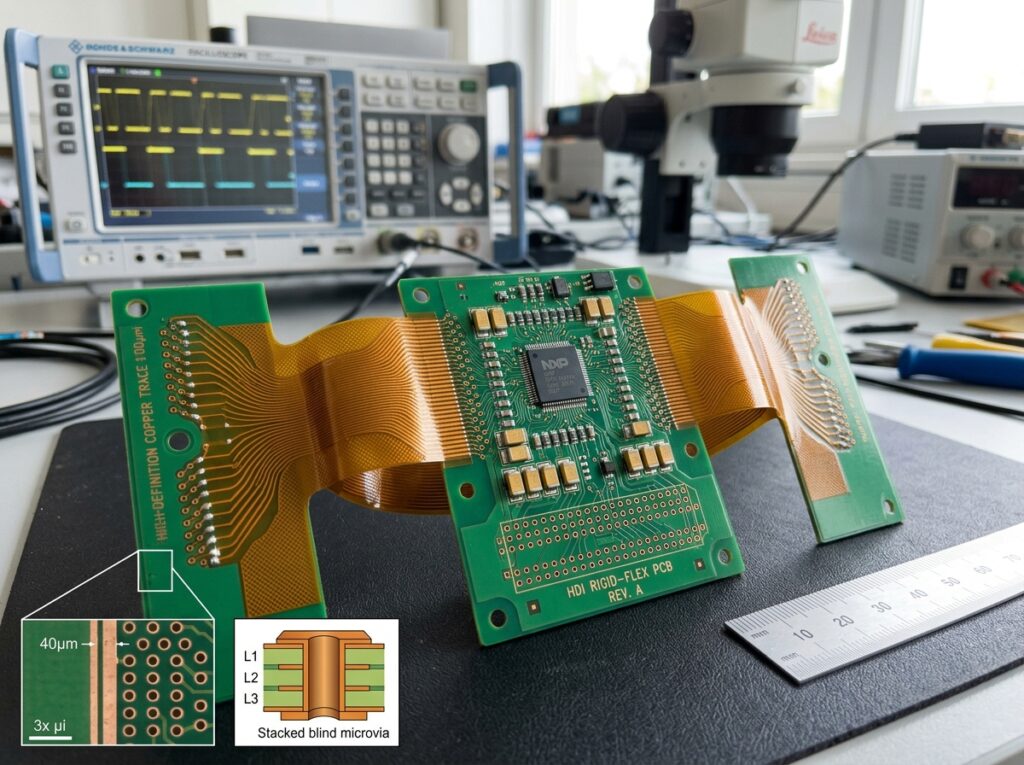
High-Frequency HDI PCB
High-frequency HDI combines laser-drilled microvias with mixed-Dk stackups so dense digital control, power delivery and low-loss RF routing coexist on one board – the architecture behind compact 5G massive MIMO and active antenna units.
- Laser microvias support fine-pitch BGA fan-out down to 0.4 mm
- Sequential lamination keeps RF layers free of via stubs
- Built for 5G AAUs, beamforming modules and compact radar front-ends
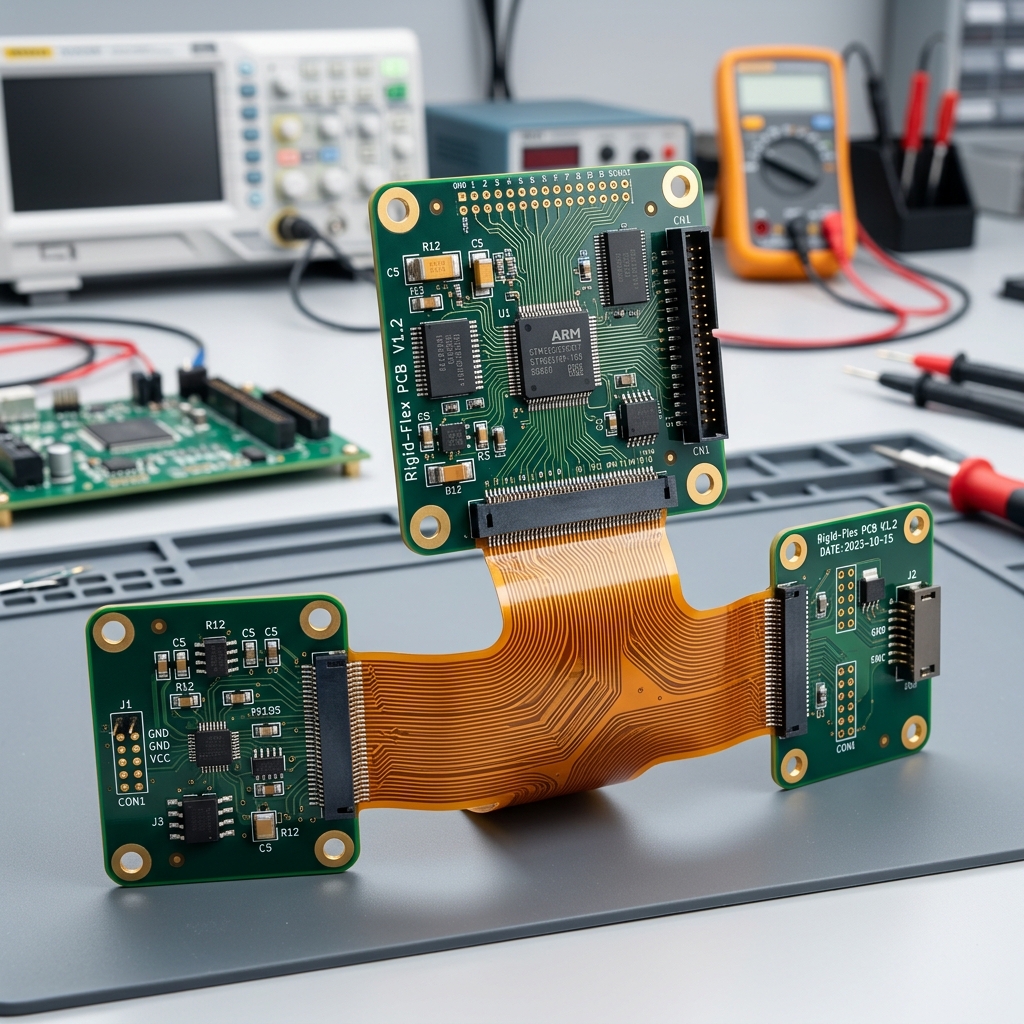
Standard FR-4 PCB vs PTFE PCB vs RO4350B Hybrid PCB
FULL COMPARISON GUIDE (SUB-6 GHZ MATERIAL & STACKUP SELECTION)
| KEY PARAMETERS | FR-4 PCB Standard Digital Board | PTFE PCB Pure Microwave Laminate | RECOMMENDED RO4350B Hybrid PCB RF + FR-4 Integration |
|---|---|---|---|
Base Material Substrate Composition | FR-4 / High-Tg FR-4 | PTFE / Hydrocarbon | RO4350B + IT-180A Hybrid |
Dielectric Constant (Dk) Dk Stability Across Lots | 4.2 - 4.6(±0.20 lot-to-lot drift) | 2.2 - 3.0(Df-driven selection) | 3.48 ± 0.05Verified per production lot |
Insertion Loss @ 3.5 GHz Signal Attenuation | 0.30 - 0.40 dB/inch | 0.10 - 0.15 dB/inch | < 0.15 dB/inch (VNA verified) |
Phase Consistency Array Beam Accuracy | ± 8° or worse(Dk drift across panel) | ± 2°(Uniform PTFE Dk) | ± 1.8° ACHIEVEDTight Phase Match on Every Channel |
Cost Structure Material Cost vs. Performance | Lowest material costRF loss budget blown | Highest material costCostly on large panels | Balanced hybrid cost30-40% Lower Material Spend(RF-grade only where needed) |
Primary Applications Best Use Cases | Consumer devices, power supplies, digital motherboards | Radar, SATCOM, base station antenna arrays | 5G small cells, massive MIMO, RRU / AAU front-ends |
| Source: Rogers Corporation laminate datasheets & IPC-6012 Class 3 fabrication standards (2026)DESIGN & SELECTION MATRIX | |||
What is a High-Frequency PCB?
A high-frequency PCB is engineered with low-loss laminates, tightly controlled impedance and matched copper profiles so RF energy reaches the antenna with minimal attenuation and phase distortion.
- Low-Loss Laminate: Rogers RO4350B or PTFE-class substrates hold Dk and Df stable across temperature, humidity and frequency.
- Controlled Impedance: Every RF trace is designed and etched to a defined characteristic impedance - typically 50 Ω single-ended or 100 Ω differential.
- Matched Copper Profile: VLP and HVLP copper foils cut conductor loss and skin-effect resistance in the GHz range.
Key Advantages
- Stable Dk 3.48 ± 0.05: Propagation delay and electrical length stay repeatable from prototype to mass production.
- Ultra-Low Df < 0.004: Less energy turns into heat, so insertion loss and thermal drift stay under control at 3.5 GHz.
- Phase Consistency ± 1.8°: Matched electrical length across RF channels keeps beamforming and array alignment accurate.
- Hybrid Cost Control: Premium RF laminate appears only on RF layers; structural layers use high-Tg IT-180A FR-4.
Why Choose RO4350B High-Frequency PCBs
Our engineering team pairs Rogers laminates with proven hybrid lamination control so RF performance stays repeatable in volume.
- Stable Dk
±0.05 tolerance held across production lots
- Low Insertion Loss
< 0.15 dB/inch @ 3.5 GHz, VNA verified
- Phase Consistency
±1.8° matched across all RF channels
- Hybrid Cost Control
RF-grade laminate only where RF lives
Core Advantages
Ultra-Low Insertion Loss: VLP copper plus the Df of 0.0037 on RO4350B keeps attenuation below 0.15 dB/inch at 3.5 GHz.
Tight Phase Matching: Tolerance-stacked substrates and uniform copper thickness hold phase error to ±1.8° on every channel.
Stable Thermal Behaviour: Dk drift stays within 0.05 from -40 °C to +85 °C, so tuning does not shift with operating temperature.
Controlled Hybrid Cost: IT-180A FR-4 carries power and ground layers, trimming material spend 30-40% versus an all-Rogers build.
Proven Case Study
How we built a Sub-6 GHz 5G small cell RF front-end board

Target Application
5G Small Cell RF Front-End Module (n78, 3.5 GHz)
Technical Challenge
Sub-6 GHz RF paths had to stay below 0.15 dB/inch insertion loss with phase matching inside ±2° across eight channels. Standard FR-4 could not hold Dk across the panel, so a hybrid stackup was the only viable route.
Structure
8-layer hybrid stackup: RO4350B on L1/L2 and L7/L8, IT-180A cores with RO4450F bondply through the middle.
Topfast Manufacturing Solution
- ✓ Material Selection: Rogers RO4350B (Dk 3.48, Df 0.0037) on all RF layers, paired with ITEQ IT-180A high-Tg FR-4 for structural and power layers.
- ✓ Copper Profile Control: VLP copper on the outer layers plus RO4450F bondply at the RF / FR-4 interface to suppress insertion loss.
- ✓ Surface Pre-Treatment: Plasma pre-treatment before plating for interlayer bond strength and residue-free hole walls.
- ✓ DFM Review: Full pre-production DFM review covering impedance targets, Dk tolerance stack and hybrid lamination flow.
Verified Results
- ✔ Insertion Loss: Measured below 0.15 dB/inch at 3.5 GHz on every panel, confirmed by S21 sweep on the vector network analyser.
- ✔ Phase Consistency: Achieved ±1.8° phase match across all eight RF channels – inside the customer’s ±2° target.
- ✔ Compliance: Fully compliant with IPC-6012 Class 3; S11 / S21 and VSWR data supplied with every production lot.
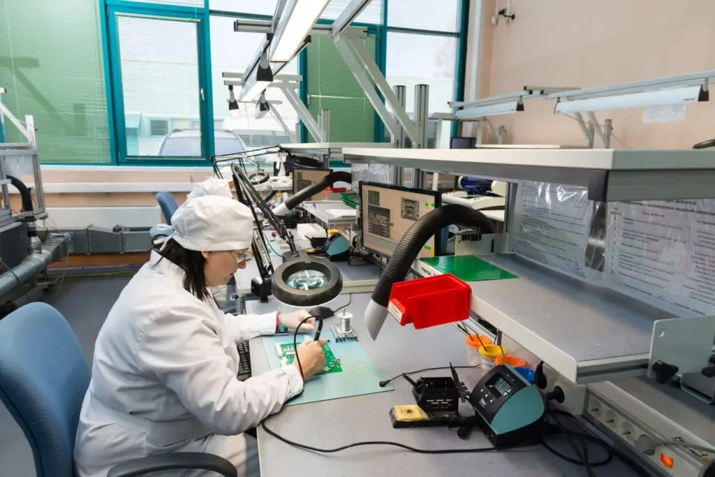
Why Choose Topfast
Engineered for Sub-6 GHz Signal Integrity and Repeatable RF Yield
Insertion Loss < 0.15 dB/inch
RO4350B with VLP copper keeps attenuation low enough for 5G small cell link budgets at 3.5 GHz.
Phase Match ±1.8°
Tolerance-stacked substrates and uniform copper thickness keep every RF channel in phase.
Dk Holding 3.48 ± 0.05
Dk verified on incoming laminate and on finished coupons, so electrical length does not drift between lots.
6 Coupons + VNA per Panel
Six impedance test coupons per panel plus full S11 / S21 VSWR verification before shipment.
Ready to Build Your 5G RF Front-End PCB?
Upload your Gerber and stackup files today for a free RF stackup review and a detailed quote within 24 hours.
Request a Quick Quote
Upload your Gerber files — DFM review & quote within 24 hours.
Engineering Capability
Technical Specifications & DFM Capabilities
| Parameter | Metric Value | Imperial Value | Feature Highlights |
|---|---|---|---|
| Layer Count | 2 - 20 Layers | 2 - 20 Layers | Hybrid RF + FR-4 Stackup |
| Dk Tolerance (RO4350B) | 3.48 ± 0.05 | Verified per lot | Repeatable Electrical Length |
| Min. Trace / Space | 0.075 mm (3 mil) | 0.003" | Fine-Line RF Routing |
| Smallest Drill (Mech/Laser) | 0.18mm / 0.127mm | 0.0071″ / 0.005″ | Microvia / Blind & Buried Vias |
| Max Aspect Ratio | 10:1 | 10:1 | Reliable Plated Through Holes |
| Finished Copper Weight | 0.5 - 2 oz (VLP / HVLP) | 0.5 - 2 oz | Low-Loss Conductor Profile |
| Impedance Tolerance | ± 5 % (typ.) / ± 3 % | 50 Ω ± 3 Ω | Tight RF Impedance Control |
Premium Substrates & Surface Finishes
- Base Material: Rogers RO4350B (Dk 3.48 / Df 0.0037), Rogers RT5880, ITEQ IT-180A high-Tg FR-4
- Bonding & Hybrid: RO4450F bondply, IT-180A prepreg, plasma pre-treatment before plating
- Surface Finishes: ENIG, ENEPIG, Immersion Silver, OSP, Selective Hard Gold
Surface Treatment Options
✔ ENIG (Electroless Nickel Immersion Gold)
✔ ENEPIG (Electroless Nickel Electroless Palladium Immersion Gold)
✔ Immersion Silver
✔ Immersion White Tin
✔ OSP (Shikoku F2)
✔ OSP (Entek)
✔ Electrolytic Soft Gold
✔ Electrolytic Hard Gold
✔ Selective Hard Gold
✔ Bondable Gold (Wire Bonding)
✔ Gold Finger (30 µin Hard Gold)
High-Frequency Fabrication Tolerances
| Parameter | Metric Value | Imperial Value |
|---|---|---|
| Dk Tolerance (RO4350B) | ± 0.05 | 3.43 – 3.53 |
| Df (RO4350B, 10 GHz) | 0.0037 | < 0.004 |
| Insertion Loss @ 3.5 GHz | < 0.15 dB/inch | VNA S21 |
| Min. Trace / Space (RF) | 0.075 mm | 0.003″ |
| Impedance Tolerance | ± 3 % | 50 Ω ± 1.5 Ω |
| Phase Consistency (8 ch) | ± 1.8° | Verified |
| Max Board Thickness | 3.2 mm | 0.126″ |
| Layer Count (Hybrid) | 4 – 12 L | 2 – 20 L |
| Min Core Thickness | 0.051 mm | 0.002″ |
| Impedance Coupons | 6 per panel | 100 % tested |
| Material Type | Example / Subtype | Function |
|---|---|---|
| RF Laminate | Rogers RO4350B | Hydrocarbon-ceramic laminate with Dk 3.48 and Df 0.0037. The default choice for Sub-6 GHz 5G RF front-end layers where both Dk stability and cost matter. |
| Rogers RT5880 / PTFE | Pure PTFE laminate (Dk 2.2, Df 0.0009) for millimetre-wave and radar designs that need the lowest possible loss. | |
| Structural Laminate | ITEQ IT-180A | High-Tg (180 °C) FR-4 used for power, ground and control layers. Provides mechanical support at a fraction of Rogers material cost. |
| Isola 370HR | Alternative high-Tg FR-4 with proven hybrid lamination compatibility and stable Z-axis expansion. | |
| MEGTRON 6 / 7 | Ultra-low-loss high-speed laminate for boards that carry both high-frequency RF and 25 / 56 Gbps serial data. | |
| RO4450F Bondply | Rogers bondply that laminates RO4350B RF layers onto FR-4 cores, holding Dk 3.3 – 3.4 across the hybrid interface. | |
| IT-180A Prepreg | Prepreg that bonds RF layers to FR-4 cores during the hybrid lamination cycle while holding Dk across the interface. | |
| VLP / HVLP Copper Foil | Very low profile foil (Ra < 2 µm) reduces conductor loss and skin-effect resistance above 3 GHz. | |
| Dielectric Families | Hydrocarbon Ceramic | RO4350B / RO4003C family. Dk 3.4 – 3.6, low Df, and FR-4-like processing for economical hybrid builds. |
| PTFE (Polytetrafluoroethylene) | Lowest Df available (0.0009 – 0.002). Requires specialised PTH conditioning and is reserved for the highest frequencies. | |
| High-Tg FR-4 | IT-180A / 370HR. Tg 170 – 180 °C, Dk around 4.3 – 4.6, ideal for structural and power layers. | |
| Ceramic-Filled Hydrocarbon | Filled laminates that raise Dk to 6.15 or 10.2 for antenna miniaturisation and impedance matching. |
FAQ
Frequently Asked Questions
A high-frequency PCB uses low-loss laminates such as Rogers RO4350B or PTFE instead of standard FR-4. The lower and more stable dielectric constant (Dk 3.48) and dissipation factor (Df < 0.004) keep insertion loss and phase error small at Sub-6 GHz, while controlled-impedance routing preserves signal integrity from the RF front-end to the antenna.
A hybrid stackup places premium low-loss Rogers laminates on the RF signal layers while using cost-effective high-Tg FR-4 (IT-180A) for power, ground and structural layers. This delivers optimal RF performance at a significantly reduced material cost – typically 30-40% lower than an all-Rogers build.
Tight Dk tolerance: Incoming laminate is selected at Dk 3.48 ± 0.05, so electrical length is repeatable between lots.
Uniform copper thickness: VLP foil with tightly controlled thickness keeps trace impedance and phase delay consistent.
Automated optical control: AOI plus etched-linewidth monitoring hold phase error to ±1.8° across all RF channels.
Our vector network analysers measure S11 (return loss), S21 (insertion loss), phase delay, impedance profiles and VSWR up to millimetre-wave frequencies. The measured data ships with every lot.
With 0.5 oz VLP copper on a 50 Ω microstrip, measured insertion loss stays below 0.15 dB/inch at 3.5 GHz. Stripline layers inside the hybrid stackup typically measure 0.10 – 0.20 dB/inch depending on dielectric thickness.
We build hybrid high-frequency boards from 4 to 20 layers, including 8- and 12-layer RO4350B / IT-180A combinations, mixed-Dk stackups with RT5880, and blind / buried via HDI constructions.
Conductor loss, dielectric loss and radiation dominate at GHz frequencies. The Df of 0.0037 on RO4350B plus VLP copper keeps both low; surface roughness usually decides the last 0.05 dB/inch.
Please send Gerber data, the stackup with Dk / Df targets, impedance requirements, laminate preference (RO4350B, PTFE or hybrid), board thickness, surface finish and quantity.
Yes. On request we supply S11 / S21 sweeps to 6 GHz, TDR impedance profiles, microsection cross-sections of the hybrid interface, and coupon data for every panel.
Our factories hold ISO 9001, ISO 14001, UL and RoHS certification, and all high-frequency boards are built to IPC-6012 Class 2 or Class 3.
Thickness follows the line width you need for 50 Ω:
2-layer RF boards typically 0.8 – 1.6 mm (0.031 – 0.063″);
8-layer hybrid standard thickness runs 1.6 – 2.0 mm (0.063 – 0.079″), commonly 1.6 mm (0.063″).
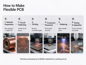
RO4350B and IT-180A cores are baked and plasma-treated, then imaged and etched on VLP copper. RO4450F bondply carries the RF layers through the hybrid lamination cycle, followed by drilling, plating, outer-layer imaging, coupon impedance measurement and VNA verification.
Common configurations include 2-layer RO4350B boards, 8- and 12-layer RO4350B / IT-180A hybrids, mixed-Dk stackups pairing RT5880 with FR-4, multi-layer PTFE builds, and high-frequency HDI with laser microvias.
Keep RF traces clear of laminate transitions, maintain a continuous ground reference under every RF line, avoid via stubs on RF layers (back-drill or blind vias), and specify impedance coupons6 per panel plus Dk / Df tolerance limits on the laminate purchase specification.