Open up any phone, laptop, medical monitor, or car ECU and you will find the same thing: a flat board, usually green, covered in tiny parts and thin silver lines. That board makes modern electronics possible. It replaces what used to be bundles of hand-soldered wires with something that can be manufactured by the millions, each copy identical to the last. The idea behind it is straightforward. The execution? PCB engineering exists as a distinct discipline for good reason.
A printed circuit board (PCB) is a flat piece of insulating material with copper pathways printed or etched onto its surface. Components like resistors, capacitors, and microchips are soldered to pads on the board, and the copper traces carry electrical signals between them. A PCB board does three things at once: it holds everything in place, routes power and data, and pulls heat away from parts that get hot. A single-layer board in a cheap toy and a 30-layer board in a server rack work on the same basic principle.
The rest of this guide explains what a printed circuit board is made of, how these boards get manufactured, the main types available, and where they show up across different industries.

What Does PCB Stand For and What Does a PCB Do?
PCB stands for Printed Circuit Board. The name is literal: circuit patterns are printed or etched onto a board. A PCB physically holds components, routes electrical power and signals between them, and dissipates heat away from parts that would otherwise overheat.
The “printing” part describes how the conductive pathways are placed onto the board. Before PCBs, electronics were assembled with point-to-point wiring. Someone soldered individual wires between each component by hand. For a simple radio with a dozen connections, this approach was fine. For a computer needing thousands of connections, this approach was impractical.
A PCB fixes this problem by embedding those connections into the board itself. The copper traces are permanent. They connect the right pins to each other every time, with no wiring mistakes, in far less space than any hand-wired version could achieve.
The mechanical function matters too. Components soldered to a PCB do not move, even when the device gets dropped, shaken, or cycled between freezing and hot. This is why you find PCBs in satellites and coffee makers alike.
For those curious about PCB manufacturing at an industrial scale, the gap between what a hobbyist can do at home and what a professional fab delivers is worth understanding.
What Is a Printed Circuit Board Made Of?
A printed circuit board is mostly a substrate called FR-4, which is woven fiberglass bonded with epoxy resin, with thin copper foil laminated to one or both sides. A solder mask layer protects the copper, silkscreen ink labels everything, and a surface finish like ENIG or HASL stops the exposed copper pads from oxidizing before soldering.
The substrate: FR-4 and alternatives
The substrate is the physical foundation of every PCB board. FR-4 owns the market because it works well enough in most situations and costs far less than anything specialized. It is stiff, it insulates, and it survives soldering temperatures without turning to mush. Those three properties cover the majority of electronic products ever made.
FR-4 is a composite. Woven fiberglass cloth gets soaked in epoxy resin and cured under heat and pressure. The glass gives it strength. The epoxy binds everything and blocks electricity. The finished sheet can be drilled, routed, and cut like any other rigid material, and it stays dimensionally stable from well below freezing to above the boiling point of water.
When FR-4 is not enough, other substrates take over:
- Polyimide: Bends without cracking. It is used in flexible circuits and anywhere the board needs to survive high heat.
- PTFE (Teflon): The go-to for microwave and RF boards. Its electrical properties stay consistent at frequencies where FR-4 becomes a signal sponge.
- Metal core (aluminum or copper): Used when heat is the main enemy. LED arrays, motor controllers, and power converters all benefit from a metal backing that pulls heat out fast.
- Ceramic: Found in things that go inside the human body or into space. Handles temperatures and power levels that would cook any polymer substrate in seconds.
Copper foil and layer count
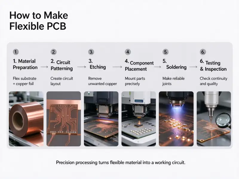
The copper starts as foil, usually between half an ounce and two ounces per square foot. It is bonded to the substrate with heat and pressure. A photoresist coating goes on next, then UV light through a photomask transfers the circuit pattern. Chemical etching strips away the unwanted copper. What remains are the traces, pads, and vias.
A single-layer board has copper on one side. A double-layer board has it on both sides, with plated holes connecting the two. Multilayer boards stack several double-layer cores with insulating prepreg sheets in between. A smartphone motherboard runs 8 to 12 layers. Some networking switches push past 30.
A deeper look at the raw materials behind these constructions reveals what PCB boards are made of, including copper foil grades, laminate types, and the trade-offs each material brings.
Solder mask and silkscreen
The solder mask is why most PCBs look green, though red, blue, black, and white show up too. Its actual job is utilitarian: cover the copper so solder only sticks to the exposed pads. Skip the solder mask, and molten solder spreads across adjacent traces, creating shorts that are a pain to find and fix.
Silkscreen is the white text you see on top. It marks where each component goes (R1, C4, U3), shows which way polarized parts face, and stamps the board with revision numbers and logos. Without it, assembly slows down and troubleshooting becomes a matter of guesswork.
Surface finishes
Bare copper oxidizes fast in open air, and oxidized copper refuses to wet with solder. Surface finishes coat the exposed pads with something that stays solderable. Here are the four you will see most often:
| Finish | What it does | Where it works best |
|---|
| HASL (Hot Air Solder Leveling) | Cheap, lasts on the shelf, surface is bumpy | Through-hole boards, quick prototypes |
| ENIG (Electroless Nickel Immersion Gold) | Dead flat, resists corrosion for years | Fine-pitch SMD, BGA packages |
| OSP (Organic Solderability Preservative) | Very flat surface, water-based, shelf life is short | High-volume consumer products |
| Immersion Silver | Good conductivity, moderate price | RF and high-frequency circuits |

How Are Printed Circuit Boards Manufactured?
PCB manufacturing starts with a design file in Gerber format, moves through substrate prep and copper patterning, then goes to etching, drilling, plating, solder mask, surface finish, and electrical test. Modern fabs hold trace widths and spacings under 0.1 mm as a routine capability, not a specialty.
Design and file preparation
Every PCB begins as a digital layout in EDA (Electronic Design Automation) software. The designer places parts, routes connections, sets the layer stackup, and picks drill sizes. The software exports Gerber files: one per copper layer, plus files for solder mask, silkscreen, and drill data. These gerbers are the standard format every fab accepts.
Inner layer processing
On multilayer boards, fabrication starts from the inside. Copper-clad laminate is cleaned and coated with photoresist. UV light shines through the photomask. Where the light hits, the resist hardens. The unhardened resist washes off, and acid etches away the exposed copper underneath. Strip the remaining resist and you have clean copper patterns on what will be buried inside the board.
Lamination
Processed inner layers get stacked with sheets of prepreg (fiberglass pre-loaded with partially cured epoxy) between them. Copper foil goes on top and bottom. The whole stack enters a lamination press. Heat plus pressure cures the prepreg and fuses everything into a single rigid board. Layer-to-layer alignment matters enormously here. Optical registration systems hold it to within a few microns.
Drilling and plating
CNC drills punch holes for vias and through-hole leads. The smallest bits are about 0.1 mm across and spin north of 100,000 RPM. After drilling, the holes get deburred and cleaned. An electroless copper bath deposits a thin conductive coating on every hole wall. Electroplating thickens that copper to spec and creates the electrical connection between layers.
Outer layer imaging and etching
The outer layers go through the same photolithography steps as the inner ones, except the plated holes need protection during etching. Fabricators either tent over the holes with resist or plug them with a non-conductive filler.
Solder mask, silkscreen, and surface finish
Solder mask gets applied as a liquid or dry film, then exposed and developed to open pads. Silkscreen goes on by screen printing or ink jet. Finally, the exposed pads get the chosen finish: HASL, ENIG, or whichever option the design calls for.
Electrical testing and inspection
Every board gets tested electrically. Flying probe machines or bed-of-nails fixtures verify that every net connects where it should and stays isolated from every other net. Automated optical inspection (AOI) catches visual defects: misaligned solder mask, traces that are too narrow, and missing pads.
The full chain from raw laminate to finished board runs through dozens of steps, each with its own tolerance budget. The PCB assembly process picks up where fabrication leaves off, turning bare boards into populated assemblies ready for functional test.
Types of Printed Circuit Boards
PCBs come in a few broad families: rigid (single-layer, double-layer, and multilayer), flexible, rigid-flex, and specialty types built around thermal or high-frequency needs. Each optimizes for a different set of constraints, and the choice ripples through the rest of the product design.
Rigid PCBs
Rigid PCBs are what most people picture when they think of a circuit board. The substrate does not bend, which is fine for anything that lives in a fixed enclosure. Consumer electronics run almost entirely on rigid boards: TVs, desktop computers, washing machines, and game consoles.
Single-layer rigid boards put copper on one side only. They cost the least and show up in the simplest products. Double-layer boards add copper on both sides with vias connecting them, roughly doubling the routing space for a small cost bump. Multilayer rigid boards stack layer after layer, routing thousands of signals in a footprint no bigger than the single-layer version.
Rigid PCB boards stay the default for most electronics projects and commercial products. The supply chain is deep, the processes are well understood, and the price is hard to argue with.
Flexible PCBs
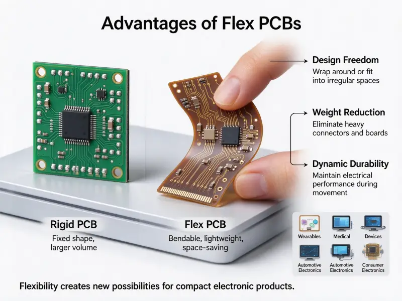
Flexible PCBs use a thin polyimide or polyester substrate that bends. Instead of forcing a designer to connect flat boards with wires and connectors, the circuit itself conforms to whatever shape the product needs. This matters in cameras, wearables, and folding phones where every cubic millimeter counts.
Flex circuits also cut connectors out of multi-board designs. Replacing a ribbon cable and two connectors with one continuous flex circuit saves space, drops weight, and removes failure points. Connectors are one of the least reliable parts in any electronic product. Getting rid of them helps the thing last longer.
Rigid-flex PCBs
Rigid-flex boards combine rigid and flexible sections in a single piece. Components that need a stable platform sit on the rigid areas. The flex sections let the board fold into a three-dimensional shape. This approach shows up in military avionics, medical implants, and premium consumer devices where the shape constraints leave no room for flat boards and jumper wires.
Metal-core PCBs
Metal-core PCBs swap the fiberglass base for aluminum or copper. The whole point is thermal management. Power components generate heat. The metal layer pulls that heat out and spreads it across the board surface. Without it, high-power LEDs, motor drivers, and voltage regulators would need bulky heatsinks or would cook themselves to death.
High-frequency and ceramic PCBs
High-frequency PCBs use substrates where the electrical properties stay predictable at microwave frequencies. FR-4 turns into a signal sponge above a few GHz. PTFE-based materials do not. Impedance control, phase stability, and insertion loss all depend on the substrate choice. Radar, satellite links, and 5G infrastructure all live in this space.
Ceramic PCBs push thermal performance further still. Aluminum oxide and aluminum nitride substrates survive power densities and temperatures that would destroy any polymer board. You find them in high-power RF amplifiers, downhole drilling tools, and implantable medical electronics.

What Is a Printed Circuit Board Used For?
Printed circuit boards go into nearly every electronic product made: phones, cars, factory robots, MRI machines, satellites, cell towers, and IoT sensors. If a product draws power and does anything smarter than turning a motor on and off, there is probably at least one PCB inside it.
Consumer electronics
Consumer electronics drive PCB production volumes more than any other sector. Smartphones, laptops, tablets, TVs, game consoles, smart speakers, and kitchen appliances all depend on them. A single flagship smartphone contains multiple boards: a main motherboard, a separate charging-port board, a camera module PCB, and often a display driver board. The main board alone might stack 10 layers into a rectangle the size of a credit card.
Automotive electronics
Cars have become one of the largest consumers of PCBs. A luxury vehicle from 2024 can carry over 100 separate PCB assemblies. They handle engine timing, transmission shifts, infotainment screens, lane-keeping cameras, adaptive cruise radar, and battery management in electric models. Automotive boards deal with temperature swings from desert heat to arctic cold, constant vibration, humidity, and road salt. The reliability bar is higher than consumer gear by a wide margin.
Industrial equipment
Factory robots, motor drives, power supplies, and process controllers run on PCBs designed for round-the-clock operation. Industrial boards often use thicker copper (3 oz or more) to carry higher currents, wider spacing between high-voltage nets, and conformal coating to seal out dust and condensation.
Medical devices
Medical PCBs go into imaging systems (MRI, CT, ultrasound), bedside monitors, surgical tools, and implanted devices like pacemakers and nerve stimulators. If the board fails, someone can die. That changes the manufacturing requirements. Medical PCB production follows ISO 13485 and IPC Class 3, which demand full traceability on every lot and far more inspection than commercial work.
Aerospace and defense
Satellites, avionics boxes, radar arrays, and missile guidance systems share one uncomfortable reality: once they are deployed, nobody is going in to swap a board. Aerospace PCBs need to survive launch shock, hard vacuum, thermal cycling from sunlight to shadow, and ionizing radiation. They get built to IPC Class 3 or military standards, often on polyimide or PTFE substrates rather than FR-4.
Telecommunications
Cell towers, fiber optic line cards, data center switches, and 5G radios all run on specialized PCBs. Signal integrity dominates the design conversation. At the data rates modern networking gear pushes, a tiny impedance bump along a trace flips bits. High-speed PCB design is a discipline unto itself, with its own simulation tools and a steep learning curve.
Bare Printed Circuit Boards: The Foundation of Electronics
A bare printed circuit board has all its copper traces, pads, vias, and surface finish applied, but no components soldered on yet. It is the starting point for assembly and the structural skeleton of the finished product.
“Bare board” distinguishes the unpopulated PCB from a fully assembled PCBA (Printed Circuit Board Assembly). Bare board testing happens before any components go on. The fabricator checks every net for continuity and every pair of nets for isolation. Finding a short or an open at this stage costs a fraction of what it costs after components are soldered down.
Bare boards also serve as the physical proof of a new design. Engineering teams order a small batch, inspect them under a microscope, probe them electrically, and only then commit to a full assembly run. Reversed footprints, missing keep-out areas, and wrong drill sizes all get caught here before they become rework nightmares.
The line between bare board fabrication and assembly is where the PCB shop’s responsibility ends and the assembly provider’s begins. Many companies do both under one roof, which simplifies things. Either way, the quality of the bare board sets the ceiling for the assembly yield.
PCB vs. PCBA: What Is the Difference?
A PCB is the bare board: copper traces and pads, no parts. A PCBA is the same board after all the components get soldered on. The PCB is the platform. The PCBA is the working circuit.
This matters when you are buying boards. Order PCBs and you get bare laminates. You still need to source components and pay someone to assemble them. Order a PCBA, and you get boards ready for testing and integration. Fabrication and assembly run on different production lines with different machines and different skill sets.
Here is the typical sequence:
- PCB design done, Gerber files exported
- Bare board fabrication
- Bare board test and inspection
- Buy components (BOM sourcing)
- Print solder paste through a stencil
- Place components with pick-and-place machines
- Reflow solder for SMD parts, wave solder for through-hole
- Inspect: AOI for everything, X-ray for BGA packages
- Functional test
- Ship assembled boards
Cost splits vary. A simple single-layer board with a few through-hole parts: the bare board might be 10 to 15 percent of the total. A dense multilayer board with hundreds of tiny SMD components: the bare board can hit 30 to 50 percent.
Frequently asked questions
How long does it take to manufacture a custom PCB?
Quick-turn prototype shops ship simple 2-layer boards in 24 to 72 hours. Multilayer boards with controlled impedance or special materials take 5 to 15 business days for standard lead times. Production volumes add queue time. Large orders can stretch to 3 to 6 weeks. Rush services exist at every level. The price jump is steep.
Can PCBs be recycled?
Yes, but it is harder than tossing aluminum cans in a bin. PCBs contain copper, gold, silver, and palladium, all worth recovering. Specialized recyclers shred the boards and use a mix of mechanical, chemical, and thermal processes to separate metals from the fiberglass. The metals get resold. The fiberglass fraction is trickier and usually ends up as filler in construction materials.
What is the minimum trace width and spacing for PCB manufacturing?
Standard consumer-grade fabs hold 0.15 mm (6 mils) of trace and space. Better shops go to 0.075 mm (3 mils). At the bleeding edge, used in semiconductor packaging and HDI boards, traces dip below 0.05 mm (2 mils). Tighter numbers cost more. They need cleaner rooms and sharper equipment, and they scrap more boards when something drifts out of spec.
What is the difference between through-hole and surface-mount components?
Through-hole parts have wire leads that poke through holes in the board and get soldered on the far side. Surface-mount parts sit flat on top of the pads. Through-hole joints are physically stronger, which is why connectors, big capacitors, and anything that gets shoved or yanked still use them. Surface-mount parts are far smaller, can go on both sides of the board, and feed through high-speed pick-and-place lines, which is how modern electronics stay affordable.