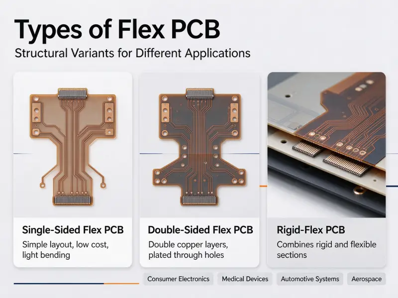
Product enclosures keep shrinking while the packages inside them keep adding pins. A 0.4 mm pitch BGA and a 100 µm trace have to coexist on a board thinner than a credit card. Laser drills, thin build-up films, and a press cycle that runs more than once make that possible, and the stack-up notes decide most of the price. Any HDI PCB manufacturer can spot an over-specified file in the layer table.
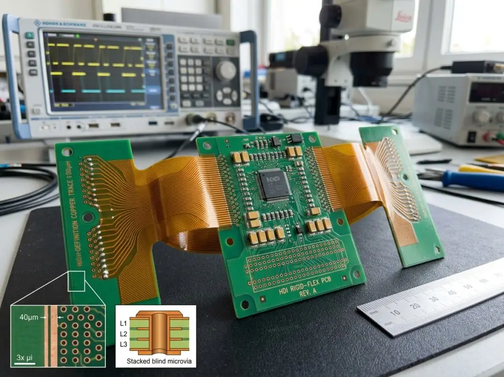
HDI stands for high-density interconnect. An HDI PCB is a circuit board built with laser-drilled microvias and finer lines than a conventional multilayer, so more connections fit into a smaller area. The density comes from the construction, not from the laminate: thin build-up layers are laminated around a core one or two at a time, and each via reaches only the layers it connects. A board that meets the microvia geometry in IPC-2226 is HDI by definition, whatever the datasheet calls it.
The rest of this guide covers how those layers are made, how to read a stackup, and where the cost accumulates.
What does HDI stand for in a PCB?
HDI is short for high-density interconnect, a term for boards whose wiring density is limited by laser drilling rather than mechanical drilling. What changed is the via, not the substrate.
A conventional multilayer resolves connections with through-hole vias plated through the full thickness. An HDI board adds its outer layers as thin dielectric films, then joins them with microvias. Once the finest pitch can no longer be fanned out with through-holes, the board has to become HDI.
The IPC-2226 thresholds that separate HDI from a standard board
The vocabulary comes from a standard, not from marketing. IPC-2226A defines a microvia as a blind or buried hole under 0.15 mm in diameter with a capture pad under 0.35 mm, an aspect ratio of 1:1 or less, and a depth under 0.25 mm from capture pad to target pad. A hole that fails those limits is a via, and the board around it is a conventional multilayer with small holes.
| Parameter | Standard multilayer | HDI |
|---|---|---|
| Via formation | mechanical drill | laser (CO2 or UV) |
| Smallest via diameter | about 0.2 to 0.3 mm | 0.05 to 0.15 mm |
| Capture pad for smallest via | via plus 0.25 mm | under 0.35 mm |
| Microvia aspect ratio | not applicable | 0.75:1 typical, 1:1 maximum |
| Line and space | 100/100 µm or wider | 100/100 µm or finer |
| Via reach | every layer | adjacent layers only |
| Lamination cycles | one | two or more |
The middle column is process capability, not standard. One fab may hold 75 µm lines on a good day and refuse them in production.
Why the through-hole via ran out of room
A through-hole via passes through every layer, so it removes a routing channel from layers that have nothing to do with the connection. The unused barrel above and below the connected layer also acts as a stub, and at multi-gigabit rates a stub reflects energy into the trace and notches insertion loss. Mechanical drilling holds only about an 8:1 to 10:1 aspect ratio, so a thick board can’t carry a small hole reliably.
What are the four main types of PCBs?
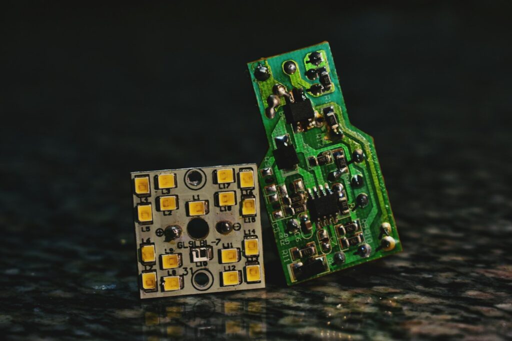
The four main types are single-sided, double-sided, multilayer, and rigid-flex. HDI is not a fifth type. It is a construction upgrade applied to the last two.
| Type | Copper layers | Construction | Where it’s used |
|---|---|---|---|
| Single-sided | 1 | tracks on one face, no plated holes | simple controls, low-cost assemblies |
| Double-sided | 2 | plated through-holes join both faces | consumer and industrial boards |
| Multilayer | 4 and up | laminated inner layers, vias between them | computing, automotive, instrumentation |
| Rigid-flex | 2 and up | rigid sections joined by flexible sections | wearables, camera modules, medical probes |
A six-layer 1+N+1 board is still a multilayer PCB, and an HDI rigid-flex is still a rigid-flex. Catalogues sometimes list HDI as a separate category, which confuses buyers, since every HDI board also belongs to one of those four families. Single-sided and double-sided boards rarely need HDI; their pin counts are low.
How the HDI PCB manufacturing process works
The process runs in stages. The core is imaged and laminated first, then build-up layers are added a pair at a time, with laser drilling, plating, and via fill between each lamination. A 2+N+2 board goes through the press three times, not once.
- Image and etch the inner layers on the core.
- Laminate the core and drill any buried vias.
- Laminate the build-up film, one side at a time.
- Laser-drill the microvias.
- Desmear the hole bottoms, then plate.
- Fill and planarize the vias.
- Repeat steps 3 to 6 for each additional build-up layer.
- Apply surface finish and solder mask, then test.
Every step after the first lamination sees a panel that has already been through one thermal cycle, and a defect found at step 8 has consumed the cost of steps 1 through 7.
Laser drilling and desmear
CO₂ lasers ablate dielectric but won’t cut copper, so the foil works as a mask and the hole lands where the pad is exposed. UV lasers cut both, which suits finer openings. Energy control is the whole trick: too little and the hole misses the target pad, too much and the pad is damaged.
Laser ablation leaves a resin smear on the target pad, and plating over the smear gives a joint that passes electrical test and opens in the field. A fab that shortens desmear gives up the reliability margin the customer paid for.
Sequential lamination and registration
Each cycle presses a panel that has already grown, and each adds its own alignment error. Fabs scales the artwork for the laminate’s expected movement and drills X-ray targets into the core, so the next layer registers what happened rather than the design intent.
Yield compounds here. If one cycle runs at 95 percent, three cycles land near 86 percent before any laser drilling is counted.
Via fill and planarization
An unfilled via-in-pad wicks solder paste down the hole during reflow. The joint starves, voids form under the component, and the failure shows up as an intermittent open after thermal cycling. Filling the via with copper or epoxy and grinding the surface flat gives the stencil a sealed pad.
This is the step most often missing from a cheap quote. Fill and planarization need extra plating, grinding, and inspection, so the cost is visible. The assembly yield lost six weeks later is not.
HDI stackup types: what 1+N+1 actually means
The notation counts build-up layers on each side of the core. In 1+N+1, the ones are microvia layers and N is the core, so a 1+4+1 board has six layers and needs two press cycles.
| Notation | Microvia layers | Example total | Press cycles | Typical BGA pitch |
|---|---|---|---|---|
| 1+N+0 | top face only | 1+4 = 5 | 2 | 0.8 mm and above |
| 1+N+1 | one per face | 1+4+1 = 6 | 2 | 0.65 to 0.8 mm |
| 2+N+2 | two per face | 2+4+2 = 8 | 3 | 0.5 to 0.65 mm |
| 3+N+3 | three per face | 3+6+3 = 12 | 4 | 0.4 to 0.5 mm |
| Any-layer | every layer pair | varies | 5 and up | under 0.4 mm |
IPC-2226 sorts the same constructions by via type. Type I has one microvia layer per side and no buried vias. Type II adds buried vias in the core. Type III has two or more microvia layers on at least one side, plus buried vias. Higher types cover passive substrates and coreless builds.
The pitch figures are rules of thumb. A 0.5 mm pitch part can sometimes route on 1+N+1 with heavy dog-bone fanout, so it pays to price both options.
Stacked vs. staggered microvias
Stacked microvias sit on top of each other, forming a vertical path. They use less lateral space, but each layer needs copper fill and planarization before the next via is drilled, and the stack concentrates thermal stress at one point.
Staggered microvias offset from layer to layer. They need no fill and spread stress but consume routing space and add inductance. Skipped vias, where one drill passes through two dielectric layers, sit in between: fewer landing pads, tighter depth control, fewer fabs willing to commit.
Rigid-flex and flex HDI
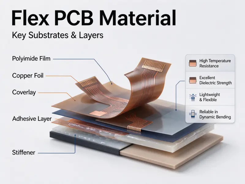
Flexible cores take microvias too, with polyimide dielectrics and reinforced plating at the via walls. Vias and stiffeners stay out of bend areas, and the coverlay opening has to clear the capture pad. A rigid-flex PCB with HDI build-up on the rigid sections is common in camera modules and medical probes.
HDI PCB design rules that decide buildability
Most HDI quotes move for reasons set during layout: a via-in-pad without fill, a stackup the fab can’t register, or a panel that wastes a third of the sheet. The factory executes the design it receives.
| Parameter | Mainstream capability | Advanced capability |
|---|---|---|
| Line and space | 100/100 µm | 75/75 µm and finer |
| Microvia diameter | 100 to 150 µm | 75 µm |
| Capture pad on a 100 µm via | 250 to 300 µm | 200 µm |
| Microvia aspect ratio | 0.75:1 | 1:1 |
| Build-up layers per side | 1 | 2 to 3 |
| Via-in-pad | plugged and capped | copper filled and planarized |
Four habits keep a design buildable:
- Keep the stackup symmetric in copper and dielectric so the panel doesn’t bow during reflow.
- Give the target pad an annular ring that survives registration error, not just the nominal drill.
- Put impedance coupons on the panel and ask for measured data, not a capability statement.
- Check the design against the fab’s rules before release. Generic checks pass features a specific laser drill can’t place.
What drives HDI PCB price
HDI pricing follows process steps and yield, not board area. Two boards of the same size can differ by a factor of two or three when one needs an extra lamination cycle and copper-filled via-in-pad.
| Cost driver | Why it costs | How a buyer controls it |
|---|---|---|
| Build-up layers | each adds press, drill, plating, inspection | start at 1+N+1 and escalate only when pitch forces it |
| Microvia count | laser drilling is serial, one hole at a time | drop unnecessary via-in-pad; use dog-bone where pitch allows |
| Panel utilization | small boards leave an unusable border | size the array to the panel, not to the drawing |
| Yield loss | a defect at the end wastes every earlier cycle | DFM review before tooling, agreed inspection plan |
| Materials | low-Dk and high-Tg laminates cost more | specify them only where impedance or thermal limits require |
| Volume | setup is amortized over the run | prototype on the simplest stackup that works |
The most useful thing to send with an RFQ is a complete stackup: layer count, dielectric thicknesses, microvia count, BGA pitch, surface finish, impedance targets, IPC class, and annual volume. Without that, the fab prices the worst case.
A low HDI quote usually means one of three things: a stackup the fab panels efficiently, a via fill step quietly left out, or a yield assumption corrected after the first lot. Only the first is good news.
When HDI is justified and when a standard multilayer is enough
Two conditions force HDI: the finest pitch can’t be fanned out with through-hole vias, or the layer count needed for routing won’t fit the available thickness with mechanical drilling. Everything else is a cost-benefit call.
| Situation | Verdict |
|---|---|
| 0.5 mm pitch BGA plus 8 layers of routing | HDI |
| Fine pitch, but routing fits in 4 to 6 layers | try dog-bone fanout first |
| High layer count driven by plane splits, not routing | revisit the stackup before buying HDI |
| Board under 1 mm thick with 10 or more layers | HDI, since build-up dielectric is thin |
| Multi-gigabit links failing on via stubs alone | backdrilling is usually cheaper |
| Large board, low annual volume | standard multilayer wins on setup cost |
Backdrilling is the most common alternative and the most common oversight. It removes the unused barrel after plating, which fixes the stub problem without changing via pitch or layer count, but it does nothing for density.
Where HDI boards are used
HDI appears wherever a package pitch, a thickness limit, or a frequency requirement rules out through-hole fanout.
- Phones and wearables: density and thickness drive the stackup, often to any-layer on the main board.
- Automotive radar and ADAS: fine-pitch processors plus thermal cycling, so via fill quality matters more than raw density.
- Medical imaging: channel count in a small head, with reliability classes that limit the via structures allowed.
- Data centre switches and optical modules: high-speed links where short stubs and thin dielectrics both help.
- Aerospace and defence: weight and layer count, with qualification testing that often rules out stacked microvias.
How to evaluate an HDI PCB board manufacturer
Judge a supplier by the equipment it owns and the documents it can produce, not by the maximum layer count on its home page. HDI is a chain of processes, and outsourcing any link adds handling and registration risk.
- Minimum laser drill diameter, in production rather than in a lab sample.
- Press capacity for sequential lamination, and how many cycles it will accept.
- Via fill method, copper or epoxy, and how the surface is planarized.
- A DFM report against IPC-2226 before tooling.
- Impedance coupon measurements from a comparable build.
- Microsection images showing plating thickness at the via wall and on the target pad, plus the IPC class stated for that construction.
A sample build answers most of these faster than an audit. Order the hardest stackup in the program, not the easiest one.

FAQ
Do HDI boards still use through-hole vias?
Yes. Most HDI stackups keep plated through-holes for connectors, press-fit parts, and power. Microvias handle dense routing on the outer layers while through-holes pass through the core. Designs with no through-holes at all are usually coreless or any-layer builds.
How thin can an HDI PCB be?
Thickness follows layer count and impedance targets. A 1+N+1 board on a thin core can be built well under a millimetre, which is why phone boards use that structure. Very thin panels are harder to handle and register, so the limit is set by the fab’s equipment.
Does HDI change assembly requirements?
It changes three things: stencil design for filled via-in-pad, paste volume on fine-pitch pads, and the reflow profile for thinner boards with less thermal mass. The assembler also needs X-ray to check voiding under BGA sites.