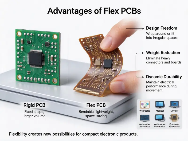
Every electronic device you use depends on one thing: a printed circuit board with components soldered onto it. The bare board itself does nothing. It is a platform. The real function happens when resistors, capacitors, integrated circuits, and connectors are placed and soldered onto it. That process is PCB assembly, or PCBA as the industry calls it. Skip this step, and no electronic product ever leaves the drawing board.
PCB assembly is the manufacturing process of soldering or mounting electronic components onto a bare printed circuit board to create a functional electronic circuit, known as a PCBA. It involves solder paste application, component placement, reflow or wave soldering, inspection, and testing. The result is a board that can process signals, regulate voltage, run firmware, and communicate with other system components.
This guide covers every part of the assembly process: what it involves, how each step works, the different technologies behind it, the people and machines that make it happen, and what to look for when you need PCB assembly services for your own project.

What is PCB assembly and why does it matter?
PCB assembly means populating a bare fabricated PCB with electronic components and forming permanent electrical connections through soldering, producing a functional printed circuit board assembly ready for integration into an end product.
A bare PCB is just fiberglass with copper traces. It has shape but no function. PCB assembly changes that. Once components are soldered on, the board becomes capable of signal processing, voltage regulation, firmware execution, and system communication.
The term “PCBA” stands for “Printed Circuit Board Assembly” and refers to the finished board after all components are attached. People often confuse PCB with PCBA. A PCB is the naked board. A PCBA is the board after assembly. The distinction matters because they arrive at different stages of manufacturing and are often sourced from different suppliers.
The role of PCB assembly in product development
Product development follows a clear sequence. Design comes first. Engineers create schematics, lay out traces, and generate Gerber files along with a bill of materials. Fabrication is next. A PCB manufacturer takes those Gerber files and produces bare boards. Assembly is the third step. An assembly house takes those bare boards, sources the components from the BOM, and solders everything together. After assembly comes testing, programming, enclosure integration, and final quality checks.
Missing or skipping any step can delay a product by weeks. Assembly is where the most value gets added to the board, and it is also where the most things can go wrong. A poorly assembled board might pass visual inspection but fail after three months in the field. Understanding the process before you engage a PCB assembly partner helps you ask the right questions and spot potential problems early.
The PCB assembly process step-by-step
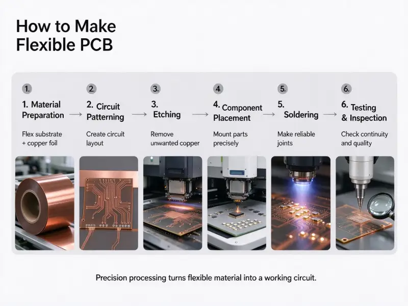
The standard PCB assembly process consists of solder paste printing, component placement, reflow soldering, inspection, and functional testing. Designs with through-hole parts add wave or selective soldering after the surface mount stage.
Every PCBA line follows the same general sequence, though specifics vary depending on board complexity, component mix, and production volume. Here is how a typical surface mount line operates.
Solder paste application
Solder paste is a mixture of tiny solder particles and flux. It gets applied to the PCB pads through a stainless steel stencil that is laser-cut with openings matching the pad pattern exactly. A squeegee blade pushes paste across the stencil, forcing it through the openings onto the pads.
Stencil design is its own discipline. Aperture size, shape, and wall smoothness all affect paste release. When stencil design goes wrong, paste deposits become inconsistent and defects multiply downstream. After paste printing, a solder paste inspection machine checks deposit volume, height, and alignment. Catching paste defects here saves significant rework cost compared to finding them after reflow.
Component placement
Pick and place machines do the heavy lifting. They take components from reels, trays, or tubes and place them onto the paste-covered pads with micron-level precision. A modern placement machine handles tens of thousands of components per hour.
The placement sequence matters. Smaller components like 0201 resistors and capacitors go first because they are light and less likely to shift. Larger parts, connectors, and BGAs go later. Component orientation is programmed from the centroid file generated during PCB design. A single misplaced polarized capacitor can prevent the entire board from powering up.
Reflow soldering
After placement, boards enter a reflow oven. The oven has multiple heating zones that gradually raise the board temperature through a controlled thermal profile with four phases: preheat, soak, reflow, and cooling.
During preheat, the board and components warm up gradually to avoid thermal shock. In the soak phase, temperature stabilizes to activate flux and remove oxides. The reflow phase peaks above the solder melting point, typically around 240 to 250 degrees Celsius for lead-free solder. The solder particles melt, wet the pads and component leads, and form metallurgical bonds. Cooling solidifies those bonds into permanent connections.
The thermal profile for each board design is unique. Too fast, and components crack. Too slow, and the flux burns off before it can clean the surfaces. Too hot, and sensitive components get damaged. Getting the profile right requires running test boards through with thermocouples attached, a process called profiling.
Inspection and testing
No board leaves a professional assembly line without inspection. Automated optical inspection compares assembled boards against the original design files, flagging missing components, tombstones, bridges, insufficient solder, and wrong polarity. X-ray inspection looks under BGAs and other hidden joints that optical systems cannot see.
Electrical testing follows inspection. Flying probe testers check for opens and shorts by probing test points on the board. For higher volumes, a bed of nails test fixture speeds up the process. Functional testing verifies that the assembled board works as intended under power.
Through-hole assembly
Not every component can be surface mounted. Large connectors, transformers, and high-power components still use through-hole technology. Through-hole components have leads that go through holes drilled in the PCB and get soldered on the opposite side.
Wave soldering is the traditional method for through-hole assembly. The board passes over a molten solder wave that contacts the bottom side, soldering all exposed leads simultaneously. For mixed-technology boards with both SMT and through-hole parts, selective soldering applies solder only where needed using a miniature fountain. Hand soldering handles the few remaining joints that machines cannot reach, typically for prototypes or very small production runs.

Types of PCB assembly technologies
The three main PCB assembly technologies are surface mount technology, through-hole technology, and mixed technology. The choice depends on component type, board complexity, and application requirements.
Surface mount technology
SMT is the dominant method in modern electronics manufacturing. Components have small metal tabs or balls instead of wire leads. They sit directly on top of pads on the board surface. SMT enables higher component density because parts can be placed on both sides of the board. It also works better at high frequencies because shorter connections reduce parasitic inductance.
The shift to SMT over the past three decades is a big reason electronics have gotten smaller and cheaper. A board that once required a dozen through-hole ICs can now be built with a single BGA package and a handful of tiny passives.
SMT has limitations. Components are harder to hand-rework because the joints are underneath the package. Thermal cycling stresses solder joints more than with through-hole parts. For products that face high vibration or extreme temperature swings, engineers often combine SMT with selective through-hole for mechanical strength.
Through-hole technology
Through-hole mounting puts component leads through drilled holes and solders them to pads on the opposite side. The resulting joint is mechanically stronger than a surface mount joint because the lead anchors through the board.
Military, aerospace, and industrial equipment still use significant through-hole content. Connectors that get plugged and unplugged repeatedly benefit from through-hole mounting. High-power components that generate heat also favor through-hole because larger leads conduct heat away from the component body more efficiently.
Mixed technology
Most real-world boards use both SMT and through-hole. A typical mixed-technology board might have all its ICs and passives surface mounted on both sides, while connectors, relays, and large capacitors are through-hole mounted. The assembly line handles SMT first, then processes the through-hole parts in a separate wave or selective soldering step.
Mixed technology costs more because it requires two different soldering processes. But in many cases, the alternative is to redesign key components around SMT packages that do not exist or to compromise on the mechanical performance the product needs. A good PCB assembly design guide helps you reduce mixed-technology overhead while maintaining quality.
Key players in PCB assembly
The PCB assembly operator
A PCB assembly operator runs and monitors the machines on the production line. Their day involves loading feeders onto pick and place machines, checking solder paste quality, inspecting boards between stations, and flagging any process drift before it turns into a batch of scrap.
The operator role has shifted significantly over the past decade. Ten years ago, operators spent most of their time manually placing components and touching up solder joints. Today they spend more time monitoring data. Modern SMT lines generate real-time metrics on placement accuracy, paste deposition, and oven profiles. The operator watches those numbers and intervenes when something trends the wrong way.
That said, the best operators still have a feel for the line. They hear when a placement nozzle sounds off. They notice a paste print that looks slightly thinner than it did ten minutes ago. Experience matters because automated systems catch known problems, but the operator catches the unknown ones.
The PCB assembly line
A PCB assembly line is a connected sequence of machines that perform each step in order: loader, solder paste printer, SPI machine, pick and place machines, reflow oven, and unloader. Some lines also include automated optical inspection inline rather than as a separate station.
Line configuration depends on product mix. A high-mix low-volume shop might run three placement machines on one line to handle the wide range of component types without constant feeder changes. A high-volume shop producing a single design might run one fast machine and optimize everything around throughput speed.
Line balancing is the art of matching each station’s cycle time so no machine becomes the bottleneck. If the printer takes 30 seconds per board but the placement machine takes 45 seconds, the line runs at the slower pace and the printer sits idle for 15 seconds each cycle. For products running in the millions of units, shaving a few seconds off the bottleneck station translates to real money.
PCB assembly services
A PCB assembly service is a company that takes customer-supplied design files, Gerbers, and a bill of materials, then sources components, assembles the boards, and ships finished PCBAs. Some services also offer design review, testing, conformal coating, box build, and logistics.
Services vary enormously in scale and capability. Some specialize in prototyping and handle runs as small as five boards. Others run high-volume production for consumer electronics where minimum orders start in the thousands. Many offer component sourcing to reduce the headache of managing long-lead-time parts.
When evaluating a service, look beyond the quote. Ask about their inspection equipment, their supply chain for components, and how they handle design changes mid-production. The cheapest quote often comes with hidden costs in rework, delays, or boards that pass electrical tests but fail in the field weeks later.

Turnkey PCB assembly
Turnkey PCB assembly is a full-service model where the assembler handles everything from component procurement through final assembly, testing, and shipping. The customer provides design files and receives finished, tested boards without managing any intermediate steps.
The alternative to turnkey is consignment assembly, where the customer buys all components themselves and ships them to the assembly house. Consignment can save money on the BOM if you already have supply agreements with component distributors. But it also means you own the inventory risk. If a design change makes a reel of expensive ICs obsolete, you eat that cost.
With turnkey assembly, the manufacturer takes on procurement and inventory management. They buy the components, store them, track shelf life on moisture-sensitive parts, and handle kitting for each production run. Many manufacturers get better component pricing than small customers because they aggregate volume across multiple clients.
When turnkey makes sense,
Turnkey works best when:
- You do not have an in-house procurement team
- Your volumes are moderate and do not justify dedicated supply chain staff
- You want a single point of responsibility for both component quality and assembly quality
- Lead time matters more than squeezing every cent out of component cost
For startups and small product teams, turnkey removes a massive operational burden. Instead of tracking 300 line items across five distributors and managing incoming inspection for every reel, you deal with one partner who handles all of that and ships you assembled and tested boards.
When consignment or partial turnkey is better
If your product uses proprietary ICs, custom-programmed microcontrollers, or parts you have negotiated special pricing on, a partial turnkey or consignment model might work better. The assembler handles standard passives and connectors while you supply the specialty components. This hybrid approach gives you control over the critical BOM items while still offloading the grunt work of buying thousands of resistors and capacitors.
Quality control in PCB assembly
Quality control in PCB assembly is not a final step. It starts long before the first board hits the line. Incoming component inspection verifies that parts match the BOM and have not been counterfeited. Solder paste inspection catches print issues before components go on. Automated optical inspection flags assembly defects before the board enters the oven. Post-reflow AOI catches soldering problems while rework is still practical. X-ray peers under BGAs. Electrical test finds opens and shorts. A functional test confirms the board does what it is supposed to do.
Each stage catches problems the previous stage could not see. Skipping any one of them pushes the detection downstream where rework costs more and some defects become impossible to fix.
Common assembly defects
Solder bridges happen when excess solder connects two adjacent pads, creating a short circuit. Tombstoning occurs when a small chip component stands up on one end during reflow because of uneven heating or pad size mismatch. Insufficient solder makes joints mechanically weak and electrically unreliable. “Component shift” means a part moved during reflow and no longer aligns with its pads.
All of these are preventable with good process control. The difference between a line that produces 99 percent first-pass yield and one stuck at 95 percent often comes down to how carefully they manage stencil cleaning intervals, paste temperature, placement nozzle maintenance, and oven profile stability.
Standards and certifications
IPC standards define what acceptable solder joints look like. IPC-A-610 is the most widely used acceptance standard for electronic assemblies. It defines three classes: Class 1 for general electronics, Class 2 for dedicated service electronics, and Class 3 for high-reliability electronics where failure is not an option.
A manufacturer that builds to Class 3 standards has tighter process controls than one building to Class 2. The solder fillet requirements are stricter, voiding limits are lower, and inspection covers more criteria. If your product goes into medical devices, aerospace, or automotive safety systems, verify that your partner can meet Class 3 requirements for the relevant portions of the assembly.
How to choose a PCB assembly partner
Choosing a PCB assembly partner involves more than comparing unit prices. The cheapest option sometimes costs more after factoring in delays, quality problems, and the engineering time you burn troubleshooting someone else’s mistakes.
Technical capability match
Your partner needs equipment that matches your board’s requirements. If your design uses 0201 passives, make sure their placement machines handle that package size. If you have fine-pitch BGAs, confirm they have X-ray inspection. If your board is 12 layers with impedance control, verify that their process can handle it without excessive warpage during reflow.
Ask for a capability checklist and compare it against your design. Many manufacturers publish these on their website. If your design pushes their stated limits, ask how they handle borderline cases. A good manufacturer tells you when your design is asking for trouble before you commit to production.
Supply chain management
Component lead times can derail a project. A manufacturer with established relationships at major distributors can often source parts faster than you can independently. They also watch for end-of-life notices and suggest alternatives before your BOM goes obsolete.
The component shortage periods from recent years showed why supply chain matters. Companies that relied on a single distributor or had no buffer stock saw production lines stop. Those with diversified sourcing and strong manufacturer relationships kept running. Ask potential partners how they managed through shortage periods. Their answer tells you a lot about their supply chain maturity.
Communication and support
The best technical capability means little if you cannot get a straight answer about lead time or a clear explanation of a quality issue. During evaluation, pay attention to how quickly they respond to inquiries, how thoroughly they answer technical questions, and whether they volunteer relevant information you did not think to ask.
A good assembly partner treats you like a long-term relationship from the first conversation. They point out potential issues in your design files instead of just quoting what you sent. They explain process choices instead of just giving you a yes or no on capability questions. Building PCB manufacturing and assembly relationships with this level of engineering support pays off across multiple projects, not just the first one.
The future of PCB assembly
PCB assembly keeps evolving. Miniaturization pushes component sizes smaller every generation. 01005 passives are now common in high-density designs. Advanced packaging technologies like system-in-package blur the line between component and board. Automation levels continue rising, with more lines running lights-out across multiple shifts.
Testing technology improves alongside manufacturing. Automated optical inspection systems now use machine learning to improve defect detection rates. Boundary scan testing catches more faults without physical access. 3D X-ray inspection handles increasingly complex stacked packages.
Environmental regulations also shape the industry. Lead-free solder is now standard in most markets. Halogen-free materials are gaining ground. Manufacturers that invest early in compliant processes gain an advantage when regulations tighten.
For product teams, staying current on assembly technology helps during the design phase. Understanding what the manufacturing side can and cannot do at scale prevents expensive redesigns later. The best approach is to involve your assembly partner early, ideally during the schematic and layout review stages, so that the board is designed for manufacturability from the start.
Frequently asked questions
What is the difference between PCB and PCBA?
A PCB is a bare printed circuit board with copper traces but no components attached. It is the platform. A PCBA is the same board after electronic components have been soldered onto it, making it a functional assembly. In manufacturing, PCB fabrication and PCB assembly are typically separate processes handled by different departments or even different companies, though some full-service manufacturers offer both under one roof.
How long does PCB assembly take?
Prototype assembly for small batches can be completed in 24 to 72 hours with expedited service. Standard lead times for small to medium production runs range from one to four weeks. The biggest variable is component availability. If all BOM items are in stock, assembly itself is fast. If a single part has a 12-week lead time, that becomes the limiting factor regardless of how fast the assembly line runs.
How much does PCB assembly cost?
Assembly cost depends on board complexity, component count, number of unique part numbers, soldering technology required, and production volume. A simple single-sided SMT board in volume might cost a few dollars per unit for assembly labor. A complex mixed-technology board with BGA components, through-hole connectors, and conformal coating can cost significantly more. Tooling charges for stencils and test fixtures add upfront costs that amortize across the production run. Most manufacturers provide a detailed quote after reviewing your Gerber files and BOM.