A printed circuit board is built in one direction. Once the design files leave the engineer’s desk, every later stage inherits what happened in the first few, and a wrong stackup or a missing drill entry will not surface until the panel is already laminated. That is why the sequence matters even if you never stand next to a plating line. It tells you which decisions are cheap to change, which ones are locked in, and where the PCB price you were quoted actually comes from.
For most teams the board itself is the output of a custom PCB manufacturing partner, so understanding the sequence is also how you read their quote. It also explains why the gap between a two-layer prototype and a twenty-layer HDI board is less about exotic technology than about repetition and tighter numbers.
A PCB is manufactured by converting design files into physical copper patterns on an insulating substrate, then bonding, drilling, plating, protecting, and testing those patterns. The order is fixed: engineering review and CAM, inner layer imaging and etching, lamination, drilling and hole metallization, outer layer imaging and plating, solder mask and surface finish, profiling, and electrical test. A double-sided board skips the inner layer and lamination stages. A multilayer board repeats them for every pair of layers in the stackup.
The sections below follow that order and flag the details that decide whether a build passes or fails.
What has to be ready before a PCB goes into production
Nothing is fabricated until the manufacturer can rebuild your design as production data. That takes a complete and unambiguous data package, a design-for-manufacturing review against the shop’s real capability, and CAM work that turns the layout into panel images, drill programs, and tooling.
Most first orders stall here rather than on the line. A layout that looks finished in the CAD tool can still be missing the layer that defines the board outline, or it can call for an impedance the chosen stackup cannot deliver. Catching that before tooling is cut costs a phone call. Catching it after lamination costs the panel.
The data package a manufacturer needs
The standard input is Extended Gerber (RS-274X) or ODB++, one file per layer for copper, solder mask, and legend, plus a separate drill file. A package a fabricator can release to the floor also carries the layer stackup with material types and copper weights, a drill table with finished hole sizes and tolerances, controlled impedance requirements and the nets they apply to, the surface finish and solder mask color, and any panel or array preference, including whether tooling rails should be added.
Design for manufacturing and CAM
Engineering compares the data against the shop’s published capability: minimum trace and space, minimum annular ring, drill-to-copper clearance, solder mask slivers, and acid traps around fine pads. This is where PCB board design decisions either survive or come back as questions. After the review, CAM turns the design into shop-floor artifacts: a panelized array sized for material yield, tooling holes and process coupons for test, and either photo tools plotted on film or direct imaging data for laser exposure.
The production stages at a glance
| Stage | What leaves the stage |
|---|---|
| 1. Engineering review and CAM | Approved data, panel images, drill program, tooling |
| 2. Inner layer imaging and etching | Inner cores carrying the circuit pattern |
| 3. Lamination | A bonded multilayer panel |
| 4. Drilling and hole metallization | Conductive paths between layers |
| 5. Outer layer imaging and plating | Finished outer copper circuitry |
| 6. Solder mask, legend, and finish | A protected, solderable board |
| 7. Profiling | Individual boards cut from the panel |
| 8. Electrical test and inspection | Verified boards cleared for shipment |
Inner layer imaging and etching
The inner layers are made by printing the circuit pattern onto copper-clad laminate with a photosensitive film, then chemically dissolving the copper you do not want.
The base material is a laminate: woven glass fabric in epoxy resin, with copper foil bonded to both sides. FR-4 is the workhorse grade, and it is what most boards are built on until frequency, temperature, or flexibility rules it out. Panels are cut to a manufacturing size, then cleaned and brushed to roughen the copper so the resist will grip it.
Copper-clad laminate and dry film
A photosensitive dry film is laminated to both sides under heat and pressure. From this point the panels are handled under yellow light, because white light would expose the film before the pattern is in place.
Exposure, development, and etching
The artwork for that layer is placed over the panel and exposed to UV light. Exposed resist polymerizes and hardens, while the covered areas stay soft. Development washes the soft resist away with a mild alkaline solution, and the acid etch that follows removes the now-exposed copper, leaving traces and pads. A final strip removes the cured resist. What remains is a core carrying one layer of the PCB circuit.
Automated optical inspection and oxide preparation
Before a patterned core is allowed into the stack, automated optical inspection compares it with the original design data and looks for opens, shorts, and conductors that have etched too thin. Finding a defect here costs one core. Finding it after lamination costs a whole board. The last step is a chemical oxidation that turns the copper dark and rough, giving the resin something to grip when the layers are pressed together.
Lamination: turning stacked layers into one board
Lamination bonds the inner cores, the prepreg, and the outer copper foils into a single rigid panel under heat and pressure.
Layup
The stack is built symmetrically around the center so the finished board does not bow. A typical four-layer build starts with copper foil, then a sheet of prepreg, then the first core, more prepreg, the second core, more prepreg, and finally the second copper foil.
The press cycle
Prepreg is glass fabric pre-impregnated with partially cured resin. Under vacuum and heat, the resin softens, flows into the gaps around the copper, then gels and cures. Pressure holds everything flat while that happens. Registration is the hard part: the cores have to stay aligned to each other while resin moves underneath them.
Trimming, targets, and shrinkage
After the press, cured resin that squeezed out of the edges is routed off. Target holes are then drilled from the inner-layer targets, and the drill program compensates for the shrink that occurred during the press cycle. Those holes become the reference for every later layer, which is why registration accuracy here largely sets the yield of the whole build.
Drilling and hole metallization
Drilling creates the holes that connect one layer to another. Plating makes those holes electrically conductive.
Mechanical drilling versus laser drilling
Mechanical drilling uses carbide bits on high-speed CNC spindles and handles through holes and standard vias in any laminate. Laser drilling takes over when the hole gets small enough that a bit would break or wander: microvias, defined as holes of about 0.15 mm or less, are laser-drilled, and in HDI builds they are often filled with paste and plated over so the next layer has a flat surface to print on.
Desmear and deburring
Drilling leaves burrs at the hole edges and a thin film of smeared resin on the hole wall. The burrs come off with an abrasive brush; the smear comes off with a permanganate solution or an oxygen plasma. Skip this step, and the plating will not adhere properly to the barrel, which shows up later as a cracked or open via.
Electroless copper and electrolytic plating
The laminated substrate is an insulator, so the hole wall must first be made conductive. Electroless copper deposits a thin conductive film over resin and copper alike. Electrolytic plating then builds that film up to the required thickness. IPC-6012, the qualification and performance standard for rigid boards, sets the minimum hole wall copper for a Class 2 board at 20 µm, measured at the thinnest point in a microsection. Class 3 raises it to 25 µm.
Outer layer circuitry: imaging, plating, and etching
The outer layers use much of the same chemistry as the inner layers, but in the opposite order: the pattern is plated up first, and the copper you do not want is etched away last.
Negative imaging
After plating, dry film is applied again. This time, the artwork is negative. The traces and pads are left uncovered, and the resin between them stays under cured resist.
Copper and tin plating
The exposed copper is plated up to its final thickness, holes included, and then a thin layer of tin is plated over the top. The tin is not part of the circuit. It is a sacrificial mask that protects the circuitry during the etch.
Strip, etch, and strip again.
The resist is stripped, the exposed copper between the traces is etched away, and the tin is removed. The difference from the inner layers is worth holding on to: inner layers are etched down from full copper, while outer layers are plated up and then protected while everything else is eaten away. Thicker copper takes longer to etch, which is one reason heavy-copper boards cost more.
Solder mask, legend, and surface finish
The solder mask covers the copper that must not be soldered, the legend identifies the components, and the surface finish protects the copper that must be soldered.
Solder mask
An epoxy-based ink is coated over both sides, imaged, developed so the pads stay open, and cured. It does three jobs: it stops solder from bridging between adjacent pads, it keeps covered copper away from oxidation and handling damage, and it narrows the touchable area to the pads the assembler actually needs.
Legend and component markings
Reference designators, polarity marks, and logos are printed by screen or inkjet. Registration matters more on dense boards, where a shifted legend can sit over a pad and confuse inspection.
Surface finish options
The finish is what turns exposed copper into something solder will wet, and it has to survive storage before assembly.
| Finish | What it is | Where it fits |
|---|---|---|
| Hot air solder leveling (HASL) | Pads coated in molten solder and blown flat with hot air | Low cost, general purpose; uneven surface, weak for fine pitch |
| Electroless nickel immersion gold (ENIG) | Nickel barrier with a thin gold layer, typically 0.05–0.1 µm of gold per IPC-4552 | Flat pads, fine pitch, long shelf life; higher cost |
| Immersion silver | Thin silver layer over copper | Flat and very solderable; tarnishes, so storage needs care |
| Immersion tin | Thin tin layer over copper | Flat, good for press-fit; limited shelf life |
| Organic solderability preservative (OSP) | Water-based organic film on bare copper | Cheapest flat option; survives several reflows, less robust in handling |
| Hard gold | Gold over nickel on edge connector fingers | Built for repeated insertions; not intended for soldering |
Profiling, electrical testing, and final inspection
Profiling separates the finished boards from the panel. Testing proves that the copper pattern matches the netlist before anything ships.
Routing, V-cut, and tab routing
A CNC router cuts the board outline for shaped or irregular boards. V-cut scores straight lines through an array so rectangular boards can be snapped apart after assembly. Tab routing leaves small bridges that hold the board in the array until depaneling. Arrays built for automated assembly usually add tooling rails and fiducials around the edges.
Flying probe and bed-of-nails testing
The bed-of-nails test uses a fixture with a pin for every net. It is fast per board once the fixture exists, which makes it the choice for volume. The flying probe test moves two or more heads to each net in turn. There is no fixture to build, which suits prototypes, high-mix work, and boards where the cost of a fixture would never be recovered. Both methods check continuity and isolation against the design data.
AOI, X-ray, microsection, and acceptance classes
Final inspection combines automated optical inspection with X-ray for hidden features such as via barrels and inner-layer alignment and microsection on sample boards to verify plating thickness. The acceptance rules come from published standards rather than from the shop’s opinion. IPC-A-600 is the visual guide to those rules and defines three product classes.
| Class | Typical products | How strict the acceptance criteria are |
|---|---|---|
| Class 1 | general electronics, simple consumer devices | Function-level; cosmetic defects tolerated |
| Class 2 | industrial controls, computers, automotive ECUs | Tight; the default for most B2B orders |
| Class 3 | aerospace, medical, defense, safety-critical systems | Strictest; voids and misregistrations that pass elsewhere are rejected |
How HDI, flexible, and metal core boards change the sequence
The steps do not change. What changes is how many times you run them and how small the geometry gets.
HDI and laser microvias
A high-density interconnect board builds its stackup in passes. One layer pair is imaged, laminated, drilled, and plated, then the next pair is added on top, using laser-drilled microvias to reach the layer below. Fine-pitch packages and thin consumer electronics would not close without this. Ten layers of HDI can take far more passes than twenty layers of standard multilayer, and the yield risk sits in the microvias and in registration between passes, which is why HDI PCB manufacturing is quoted and scheduled differently from standard multilayer work.
Flexible and rigid-flex
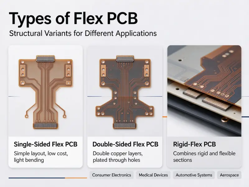
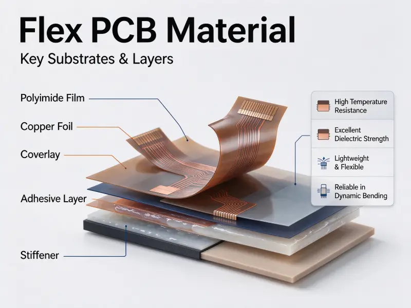
Flexible circuits use a polyimide base rather than glass-filled epoxy and a coverlay film instead of a solder mask, so the board can bend without cracking. Rigid-flex combines flexible cores with rigid outer sections in one stackup. A minimum bend radius is specified in the design, and the finished part is only as reliable as that rule allows.
Metal core and ceramic substrates
Where heat matters more than cost, the substrate changes. A metal core board uses an aluminum or copper base with a thin dielectric layer, which moves heat out of the board instead of letting it sit under the components. Ceramic substrates push that further into high-frequency and high-temperature work. Both change the etch chemistry, the drilling method, and often the surface finish, but the sequence of stages stays recognizable.
Are PCBs easy to manufacture?
A two-layer board with 0.2 mm traces and standard vias is routine work for an established shop. A twenty-layer HDI board with fine traces, laser microvias, and controlled impedance on most nets is not, and it will be quoted, scheduled, and inspected differently.
Where boards get hard to build
Difficulty is not one variable. It is a cluster of them, and they interact.
- Trace width and spacing: finer copper is harder to etch accurately and drops yield
- Layer count: every pair adds imaging, lamination, and drilling passes
- Hole wall copper: thicker plating in a smaller hole is harder to deposit evenly
- Layer-to-layer registration: the tolerance shrinks as the stack grows
- Aspect ratio: board thickness divided by drill diameter; deep, narrow holes are harder to plate
- Impedance control and back-drilling: extra process steps and extra testing
What drives PCB price and lead time
PCB price follows yield and process time rather than any single parameter, which is why two quotes for the same Gerber files can differ.
| Factor | Direction of the effect |
|---|---|
| Layer count | More layers, more imaging, lamination, and drilling passes |
| Board size and panel utilization | Poor nesting wastes material and raises cost |
| Base material | FR-4 is the baseline; high-frequency and ceramic grades cost far more |
| Surface finish | OSP and HASL sit at the low end; ENIG and hard gold cost more |
| Trace, space, and tolerances | Tighter limits lower yield, so unit price rises |
| Order quantity | Tooling and engineering are spread across the run |
| Lead time | Expedited scheduling costs more than standard |
FAQ
How long does it take to manufacture a PCB?
Lead time is quoted per order, and it depends on layer count, material availability, finish, and whether the shop has a free slot on an expedited line. Engineering review, tooling preparation, and material procurement all happen before the first panel enters the line, so a firm date only means something after the data package has been accepted. Simple boards on standard FR-4 with a common finish move through the fastest. Anything that needs a special laminate, controlled impedance testing, or several lamination passes adds time that cannot be compressed by asking for it.
What is the difference between PCB manufacturing and PCB assembly?
Manufacturing, or fabrication, produces the bare board: copper patterns, drilled and plated holes, solder mask, and finish. Assembly takes that bare board and attaches components, using solder paste and reflow for surface-mount parts or through-hole soldering for parts that need mechanical strength. They are separate processes, often at separate facilities, and they are judged against different standards. Bare boards are inspected against acceptance criteria for bare printed boards; assembled boards are inspected against criteria for electronic assemblies.
Can a PCB be manufactured in small quantities?
Yes. Prototype quantities are made by sharing panel space with other orders, so a five-piece run is practical. What changes with quantity is the economics, not the process. Engineering, tooling, and panel setup are charged against a small number of boards, so unit price falls as the order grows. Very small runs also lose access to some testing methods, because a dedicated test fixture cannot be justified for a handful of boards, and a flying probe test takes longer per board.