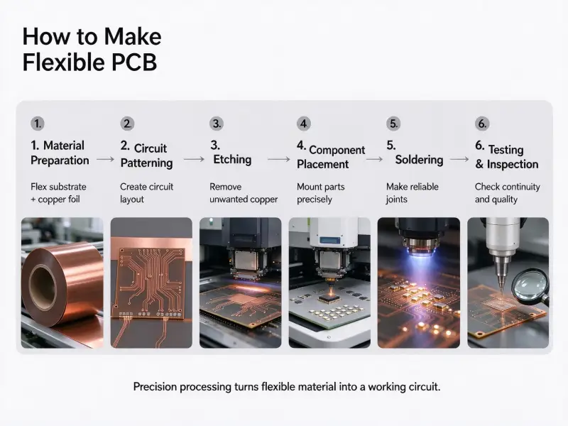
Ask ten people how to make a circuit board, and you get ten answers, because the phrase hides three separate jobs. One is drawing the layout. Another is turning it into fiberglass with copper on it. The third is attaching components until something switches on. Very little of what sits inside a phone gets made on a bench. It comes from a certified PCB PCBA manufacturer running plating lines, drilling systems, and inspection equipment under process control.
You make a circuit board in three stages: create the design files, fabricate the bare board, then assemble the components. The design stage you can do yourself with free layout software and a few evenings of practice. The other two usually go to a fabrication and assembly supplier, because a home setup cannot plate the inside of a hole, register several layers at once, or hold tight tolerances across a batch.
Everything below follows that order.
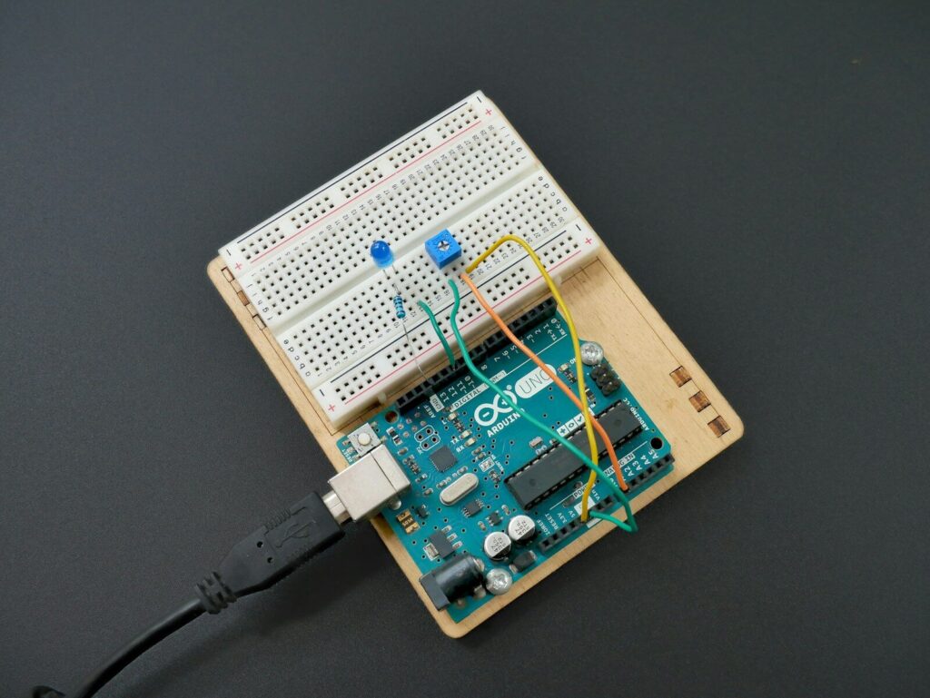
What making a circuit board actually involves
Three deliverables sit between an idea and a working board: manufacturing files, a bare board, and an assembled board. Each has a different owner, a different tool set, and a different way of going wrong.
| Stage | What it produces | Who normally does it? | How it fails |
|---|---|---|---|
| Design | Schematic, layout, Gerber, and drill files | You, in layout software | Open nets, footprints that do not match the parts |
| Fabrication | The bare board: traces, holes, solder mask | A board house | Features too fine to etch, wrong stack-up |
| Assembly | Components placed and soldered | An assembly supplier, or you with an iron | Reversed parts, cold joints, bridges |
The design files behind every board
Every printed circuit board (PCB) design starts with a schematic that names the components and says what connects to what. Layout comes next: place the parts inside a board outline, then route copper between the pads that must talk to each other. A design rule check at the end catches unconnected nets, overlapping copper and clearances that are too tight.
Free and commercial packages both work, and the choice matters less than it looks, because they export the same file formats. Circuit board design rewards dull habits: short return paths, power traces wide enough for the current, and mounting holes that line up with the enclosure.
Where a bare board ends and a PCBA begins
A fabricated board with nothing on it is a bare board, and it does nothing until parts are attached. Once components are placed and soldered, the result is a printed circuit board assembly, or PCBA. Fabrication and assembly are separate services with separate prices, lead times, and often separate suppliers.
Can you make a circuit board at home?
Yes, for simple single-sided or double-sided boards with through-hole parts and generous spacing. No, for multilayer boards, fine-pitch surface mount, or anything that needs plated vias. Home fabrication is a real skill, but its ceiling is set by physics rather than effort.
Toner transfer and chemical etching
The classic route exports the copper layer as a mirrored image and checks it prints at exactly 1:1, because a scaling error of a few percent makes an IC footprint useless. The layout goes onto glossy transfer paper, gets pressed against a cleaned copper-clad board with an iron or laminator, and the paper is peeled away. The toner left behind becomes the resist, and the board goes into an etchant. Ferric chloride and ammonium persulfate are the usual choices: both dissolve exposed copper and leave the traces. After rinsing, you strip the toner, drill the holes, and solder the parts.
Control is the trade-off: under-etch and copper bridges survive between traces; over-etch and traces thin while pads lift. Used etchant is chemical waste and should never go down a household drain.
CNC isolation routing
Milling skips the chemistry. A desktop machine cuts away the copper the traces do not need, then drills and cuts the outline in the same setup, which suits an office or a classroom. The limit is the tool: an end mill can only cut a gap as narrow as its own diameter, which hurts fine-pitch packages, and it cannot plate a hole.
The capability gap you cannot close on a bench
| Feature | Home bench | Production fabrication |
|---|---|---|
| Trace and gap width | Wide features only | Fine features routine |
| Layer count | One or two | Four, six, and up |
| Vias | Unplated, or wire links | Plated, blind, and buried |
| Solder mask and silkscreen | Optional, hand-applied | Photolithographic and aligned |
| Surface finish | Bare copper or hand-tinned | HASL, ENIG, OSP, and others |
| Batch consistency | Varies from board to board | Controlled and inspected |
Plated through-holes are the hard boundary. Plating a hole wall means chemically depositing a thin conductive layer, then thickening it electrically, which takes tanks, chemistry, and current control. Layer registration is the second barrier: pressing inner layers and prepreg together under heat and pressure is not a bench operation.
DIY or fabrication house: how to choose
Match the route to the board, not to your mood. If the design fits one or two layers with through-hole parts and you need a couple of pieces, home fabrication works. Fine-pitch parts, more than two layers, controlled impedance, or more than a handful of units all point to a fabrication house.
| Your situation | Sensible route |
|---|---|
| One or two layers, through-hole parts, a learning project | Home etching or CNC |
| A double-sided board you need the same day | Desktop CNC |
| Four or more layers | Fabrication house |
| Fine-pitch surface mount, BGA, impedance-controlled nets | Fabrication house |
| More than a few identical boards | Fabrication house |
| A product that must pass a customer audit | Fabrication house, standards in writing |
Cost and time, once you count everything
DIY looks cheap because of the visible inputs. The hidden ones change the arithmetic: consumables burn whether or not the board works, drill bits snap, a failed transfer means starting over, and chemical disposal recurs.
Ordering moves the cost into engineering time, and figures depend on layer count, copper weight, size, finish, and quantity, so every quote is specific to the design.
When outsourcing is the only sensible option
Plated vias, blind and buried vias, impedance control, and multi-layer registration all need equipment, no home setup replicates. Add a certification requirement, and the question answers itself, because printed circuit board manufacturers work to published standards and can supply the test records an audit asks for.
Selecting the printed circuit board material
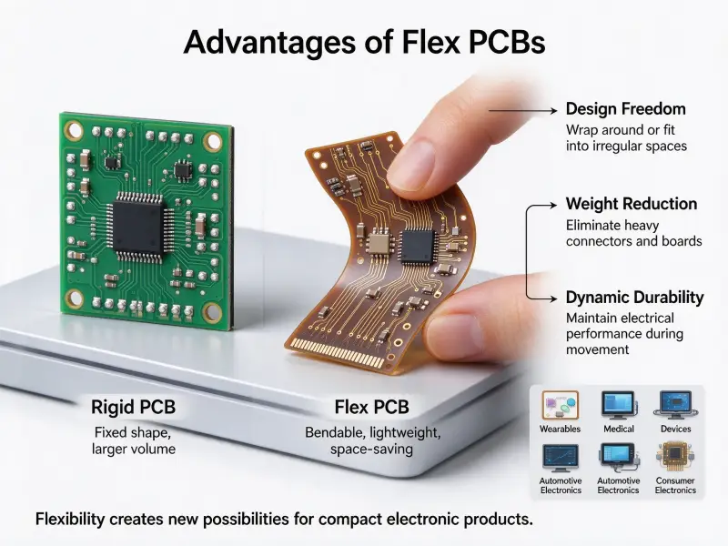
For most projects the printed circuit board material is FR-4, a woven glass and epoxy laminate, at 1.6 mm finished thickness with 1 oz copper. You change the laminate only when the application forces it: heat, flexing, high frequency, or high current.
| Parameter | Common default | Why you would change it |
|---|---|---|
| Finished thickness | 1.6 mm | Thinner for tight enclosures, thicker for heavy connectors |
| Copper weight | 1 oz, about 35 µm | 0.5 oz (about 17.5 µm) for fine lines, 2 oz (about 70 µm), and 3 oz (about 105 µm) for current |
| Laminate | Standard FR-4 | Higher glass transition for lead-free assembly, other laminates for heat or RF |
| Surface finish | HASL or ENIG | Flatness for fine-pitch pads, shelf life, wire bonding |
Copper weight is the parameter people under-specify. It is quoted as weight per square foot, so 1 oz is roughly 35 µm, and anything above 3 oz counts as heavy copper. Heavier copper carries more current and spreads heat but etches slower and costs more, so 1 oz stays the default for signal and control boards.
When FR-4 is the wrong substrate
| Substrate | What it gives you | Typical use |
|---|---|---|
| Polyimide | Flexibility and high-temperature tolerance | Wearables, flex and rigid-flex, automotive |
| Metal-core | Heat spreading through an aluminum base | LED lighting, power supplies, motor drivers |
| Ceramic | High thermal conductivity, stable dimensions | Power modules, sensors, high-temperature circuits |
| High-frequency laminate | Low signal loss, stable dielectric constant | RF, antenna, microwave links |
FR-4 wins whenever the board is flat, runs at ordinary temperatures, and carries modest current. Step away when one of those fails, and let the thermal requirement pick the material.
Design rules and tolerances that set the limit
Four numbers decide whether a design is manufacturable and what it costs: minimum trace width, minimum gap between traces, minimum annular ring around each hole, and minimum copper-to-edge distance. Set them from the fabricator’s capability list, not from whatever the layout tool allows.
Layout software will happily draw features nobody can etch, which is why capability sheets exist. Fabricators publish the lowest supported trace and spacing, the smallest drill size, and a set of tolerance bands. Ignore them, and the design comes back as a question or a price increase rather than a board. Copper-to-edge clearance is the one people forget, because outlines are cut rather than molded.
Clearance and creepage are safety numbers, not layout preferences.
Clearance is the shortest air path between two conductors; creepage is the distance along the board surface. They behave differently because air and laminate break down at different rates, and contamination or humidity degrades the surface path first. On low-voltage digital boards the difference rarely matters, but on anything switching mains or higher, spacing is a safety requirement.
This is where published standards earn their keep. IPC-2221 is the generic design standard covering spacing, trace width, and via rules. IPC-6012 states the performance requirements a finished rigid board must meet, and IPC-A-600 defines what counts as acceptable, sorting products into Class 1, Class 2, and Class 3 by the consequence of failure.
What to send before you order
A fabricator needs a complete, self-consistent package: Gerber files for every layer, an NC drill file, a stack-up description, and your written specification. For assembly, add a bill of materials and a pick-and-place file. A missing file is what turns a two-day job into a week of correspondence.
| File | What it defines |
|---|---|
| Gerber, one per layer | Copper, solder mask and silkscreen, with layers named clearly |
| NC drill file | Hole positions and sizes, matching the pads in the copper |
| Stack-up description | Layer order, dielectric thickness and copper weight |
| Bill of materials | Part numbers, values, references and acceptable substitutes |
| Pick-and-place file | Component position and rotation, for assembly orders |
| Specification sheet | Thickness, finish, tolerance and standards, in writing |
DFM questions that change price and lead time
Ask before ordering. What is your minimum trace and spacing, and does my design meet it? What is the smallest finished hole size? Will the boards be panelized, and does my outline leave enough material between parts? Do you supply the stack-up for impedance control, or do I? What test records come with the boards, and are they in the price?
Assembly and testing: when the board becomes a product
A bare board is finished when it passes an electrical test, but a product exists only after components are placed and soldered. Assembly runs one of three ways: surface mount, through-hole, or a mix. With no reflow setup, hand the board and the BOM to a partner for faster PCB assembly and keep your own time for design work.
SMT, through-hole, and mixed assemblies
Surface mount assembly prints solder paste through a stencil onto the pads. A placement machine drops components onto the paste, and a reflow oven melts it on a controlled profile: gradual ramp, short peak, and controlled cool-down. Too fast and parts tombstone; too hot and plastic connectors deform.
Through-hole assembly suits connectors, transformers, and anything needing mechanical strength, soldered by hand in small runs or over a wave in larger ones.
Inspection and first power-up
Automated optical inspection compares every board against the original data and flags missing parts, bridges, and misalignment, though it cannot see under a ball grid array, which is why X-ray exists. The electrical test then checks that every net conducts and that nothing which should be separate is connected.
Before applying power, check continuity across the power rails, then bring the first board up on a current-limited supply rather than a wall adapter.
FAQ
Can I make a multilayer circuit board at home?
Practically no. Multilayer work means laminating inner layers together with prepreg under heat and pressure, then plating the holes that connect them, and that alignment has to hold across the whole panel. Crude four-layer boards have been made by hand, but the yield is low and the effort rarely beats ordering a small run.
Do I have to solder the components myself?
No. Bare-board fabrication and assembly are separate services, and many suppliers offer both. A common approach is to order five bare boards to check the layout, then order the same design assembled once it is confirmed. It costs slightly more, but it catches footprint errors before anyone buys components.
How do I know my design is ready to order?
Three checks catch most problems. Run the design rule check with the fabricator’s own limits loaded, not the tool defaults. Print the layout at 1:1, lay the real components on the paper, and confirm pin pitches, pad sizes, and connector orientation. Then verify that the drill file and the copper layers agree, so every pad has a hole and every hole has a pad.