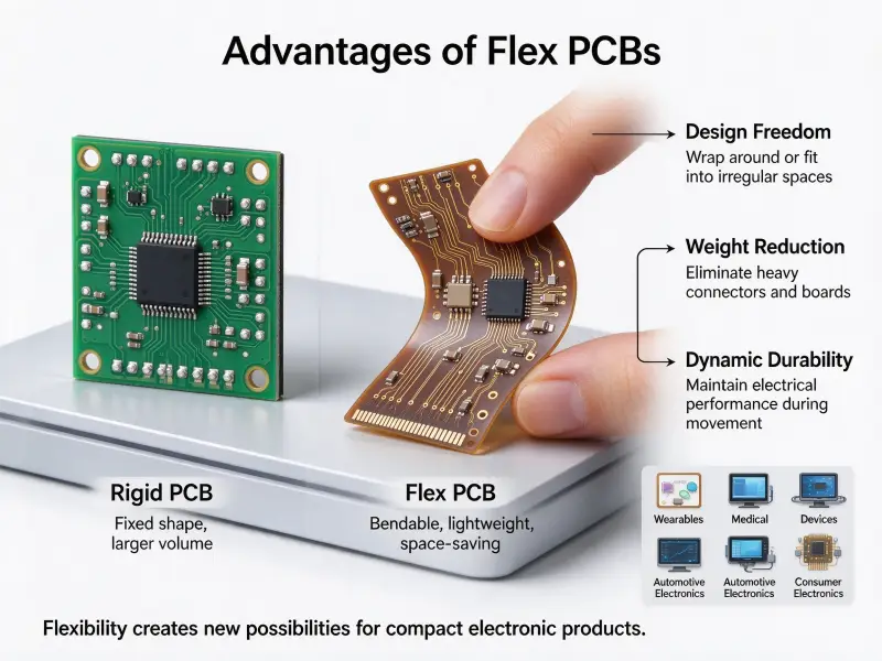
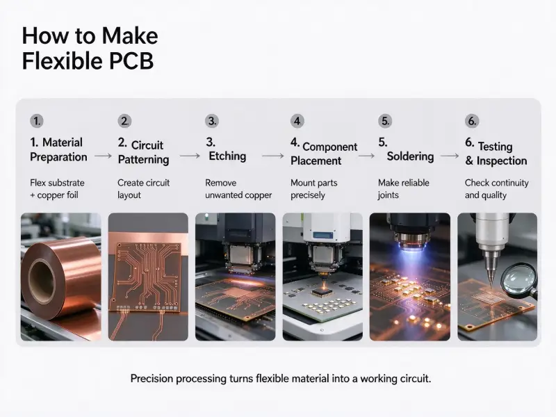
Every electronic product starts with a printed circuit board (PCB), and every PCB carries risk. A hidden solder void under a chip, a trace etched too thin, or a contaminated surface can pass a quick visual check and still fail six months later in the field. By then, the cost is no longer one board. It is a returned shipment, a failed certification, or an unhappy customer. That is why testing sits at the center of quality control for printed circuit board manufacturers and their buyers.
Printed circuit board testing is the combination of visual, electrical, and reliability checks used to confirm that a bare board or a printed circuit board assembly (PCBA) matches its design, meets industry standards, and works as intended before it ships. The seven methods used most often are in-circuit testing, functional testing, automated optical inspection, X-ray inspection, flying probe testing, boundary scan testing, and ROSE testing. Which ones your project needs depends on production volume, board complexity, and the risk profile of the end product.
This guide walks through each method, what it costs, the standards behind it, and how to pick the right mix for your next order. If you want a simpler, bench-level walkthrough for a single board, the How to Test PCB guide covers that separately.
What Is Printed Circuit Board Testing?
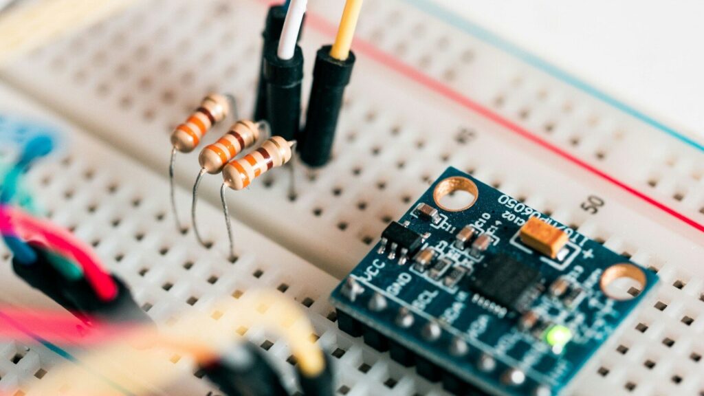
PCB testing is the process of verifying a board against its design data and accepted industry standards at the bare-board stage, after assembly, or both. It catches defects introduced by printed circuit board designs, raw materials, and manufacturing steps before the product reaches the customer.
Testing applies to two different objects, and the distinction matters when you talk to a supplier. A bare board has traces, vias, and pads but no components. A printed circuit board assembly has all components soldered in place and can actually be powered up. Bare-board checks focus on the copper: continuity, isolation between nets, impedance, and dimensional accuracy. Assembly-level checks focus on solder joints, component placement, and whether the finished circuit behaves the way the design says it should.
Defects also come from different sources. Some trace back to printed circuit board design issues, such as test points that are impossible to reach or a layout that packs components so tightly that probes cannot access them. Others trace back to printed circuit board material problems, such as laminate with a low glass transition temperature or copper with poor peel strength. Good testing plans account for both, because a board can be electrically perfect on day one and still fail in the field if the material was wrong.
Why PCB Testing Matters Before Volume Production
Testing matters because the cheapest place to find a defect is before it multiplies. A fault caught on a prototype costs a design tweak; the same fault caught after 10,000 units are built costs scrap, rework, and delayed shipments. For regulated industries, testing is not optional at all. Aerospace and medical customers work under quality systems that require documented verification of each part at defined stages of production.
Testing also protects the buyer, not just the manufacturer. When you order from an overseas supplier, your main quality control is the testing regime written into the purchase order. A supplier who runs AOI on every panel, X-rays every BGA, and functionally tests finished assemblies can show you data instead of promises.
Prototype Testing
Prototype testing answers one question: can this design be built and does it work? Engineers push early boards past normal operating conditions to learn where they break. Finding a thermal problem at this stage means a layout revision. Finding it after mass production means a recall. Most teams also use prototypes to validate test procedures themselves, so the production line starts with known-good test programs.
Manufacturing Testing
Manufacturing testing answers a different question: did this batch come out right? Instead of stressing boards to their limits, production testing repeats fast, well-defined checks on every board or on a defined sample. The goal is process control. If AOI suddenly flags more placement errors than usual, something upstream has drifted, and the line gets corrected before a full shift of scrap is produced.
What Are the 7 Types of PCB Testing Methods?
The seven methods used most often are in-circuit testing (ICT), functional circuit testing (FCT), automated optical inspection (AOI), X-ray inspection, flying probe testing, boundary scan testing, and resistivity of solvent extract (ROSE) testing. They are not competitors. Each one sees a different class of defect, and mature production lines stack several of them.
| Method | What It Finds | Stage | Best Fit |
|---|---|---|---|
| In-circuit testing (ICT) | Shorts, opens, wrong component values | After assembly | High volume |
| Functional testing (FCT) | Overall circuit behavior against spec | End of line | All volumes |
| Automated optical inspection (AOI) | Placement errors, visible solder defects | During assembly | All volumes |
| X-ray inspection | Hidden joints, voids under BGAs | During/after assembly | Complex and multilayer boards |
| Flying probe testing | Shorts, opens, component values without a fixture | Prototype to low volume | Low and medium volume |
| Boundary scan testing | Trace and interconnect faults in dense digital boards | After assembly | High-density digital designs |
| ROSE testing | Ionic contamination from flux residues | After assembly/cleaning | Boards that must resist corrosion |
In-Circuit Testing (ICT)
ICT uses a bed-of-nails fixture that presses dozens of spring pins against test points on the board. Each pin measures one node, so the tester can check every resistor, capacitor, and diode individually, even in a fully assembled circuit. The method is fast, often finishing a board in one or two minutes, and it pinpoints the exact component that failed. The trade-off is the fixture: it is custom-machined for one board design and can take weeks to build, which is why ICT pays off mainly on high-volume runs where the fixture cost is spread across thousands of units.
Functional Circuit Testing (FCT)
Functional testing powers the finished assembly and checks whether it actually does its job: does the sensor board output the right signal, and does the power supply hold its voltage under load. Testers connect through edge connectors or probe points and run a program that mimics real operating conditions. FCT usually returns a simple pass or fail, which makes it a strong final gate but a weak diagnostic tool. When a functional test fails, other data, such as ICT results, is needed to locate the cause.
Automated Optical Inspection (AOI)
AOI places cameras along the assembly line and compares high-resolution images of every board against a golden reference. It catches tombstoned components, bridged solder joints, missing parts, and misaligned placements in seconds, with no contact and no stress on the board. Its limits are physics: cameras only see what is visible. A joint hidden under a chip is invisible to AOI, and shiny surfaces occasionally trigger false calls, so programs need periodic tuning. In practice, AOI is the first and cheapest net that catches the majority of placement and surface solder defects.
X-Ray Inspection
X-ray inspection sees through the package. Because solder absorbs X-rays far more than plastic or silicon, the resulting image shows the shape and quality of joints that no camera can reach, including those under ball grid array and quad flat no-lead packages. It reveals voids, bridges, and insufficient solder inside hidden joints, and it can verify the quality of plated through-holes in dense multilayer boards. The method is slower than AOI and needs a skilled operator to read the images, so many factories reserve it for the components where hidden failure would be most expensive.
Flying Probe Testing
Flying probe testing is ICT without the bed of nails. Two or more movable probes travel across the board under software control and take the same kinds of measurements, but no custom fixture is needed. A new test program can be ready in hours instead of weeks, and a design change only means updating the program. That flexibility makes flying probe the standard choice for prototypes and low-volume builds. The cost is speed: testing takes minutes per board rather than seconds, so it stops making economic sense once volumes climb into the tens of thousands.
Boundary Scan Testing
Boundary scan, standardized as IEEE 1149.x and often called JTAG, works around a simple problem: on a dense digital board, many nets are physically unreachable by any probe. The method builds test cells into the chips themselves. Those cells let the tester drive and read signals across the interconnects between devices, checking for shorts and opens in traces the probes never touch. It also supports memory debugging, firmware programming, and system-level checks, which is why teams working with high-pin-count processors rely on it heavily.
Resistivity of Solvent Extract (ROSE) Testing
ROSE testing measures cleanliness. Boards are washed after soldering, but flux residues can remain, and ionic contamination draws moisture, causes corrosion, and creates leakage currents that show up as intermittent failures months later. In a ROSE test, the board soaks in a solvent, and the tester compares the solvent’s resistivity before and after. A large drop in resistivity means contamination came off the board. The test is quick and inexpensive, which is why it remains a common acceptance check for assemblies that must survive humid or corrosive environments.
How Much Does a PCB Test Cost?
There is no single price for a PCB test. Costs run from a few dollars per board for high-volume in-circuit testing to tens of dollars per board for low-volume flying probe work, plus setup charges that range from hundreds to tens of thousands of dollars. The ranges below are industry estimates drawn from published PCB test cost comparisons (checked 30 September 2026); actual quotes vary with board complexity, test coverage, and region.
| Method | Typical Setup Cost | Typical Per-Board Cost | Most Economical At |
|---|---|---|---|
| Flying probe | $500–$2,000 (programming only) | $5–$20 | 1–1,000 units |
| ICT | $10,000–$20,000 fixture | $1–$5 | 10,000+ units |
| AOI | Line equipment, amortized | Low per-unit | All volumes |
| X-ray | Equipment or outsourced per lot | $5–$15 per unit | Critical components only |
| Functional test | $2,000–$10,000 rig development | $5–$25 | End-of-line, all volumes |
What Drives the Cost
Three factors dominate. Volume is the biggest: setup costs are fixed, so a $15,000 ICT fixture that looks absurd on 200 boards becomes cheap on 20,000. Board complexity is second, because fine-pitch parts, HDI layouts, and dense multilayers need slower tests and more programming time. Test coverage is third. Testing every net on every board costs far more than a sampling plan, and for a mature product with a stable process, many manufacturers and buyers agree on statistical sampling instead of 100% inspection. The right level depends on what a failure would cost you in the field, which is a question worth asking before you request a quote.
How Do I Test a PCB with a Multimeter?
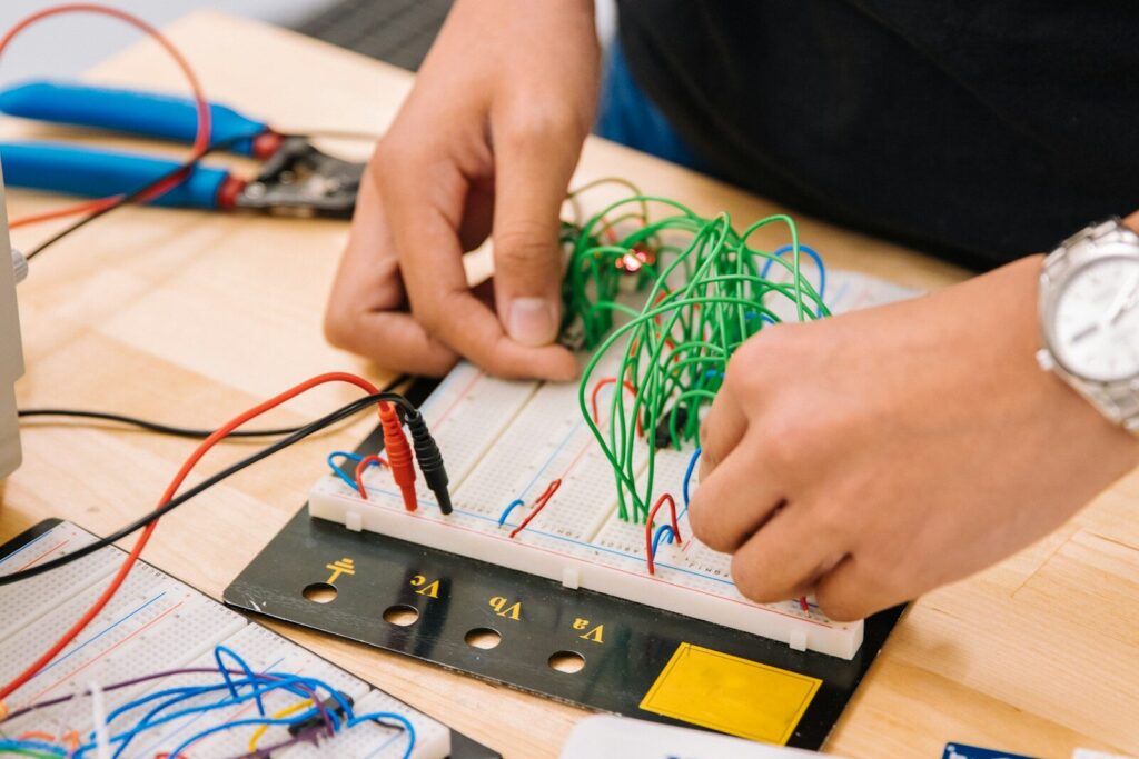
A multimeter verifies the basics: continuity, shorts, and component-level voltages. It is a diagnostic tool for a single board, not a production quality check. Set the meter to continuity or resistance, and work with the board powered off unless you are measuring voltages.
Basic Multimeter Steps
- Power the board down and discharge any capacitors before touching probes to it.
- Check power and ground for shorts by measuring resistance between the two rails. A reading near zero ohms points to a short somewhere on the board.
- Test suspected traces for continuity by probing both ends of the copper path. A digital display reading close to zero means the trace is intact; an open reading means it is broken.
- Verify individual components, such as resistors and diodes, against their expected values, ideally with at least one probe lifted so surrounding circuitry does not skew the reading.
- Power the board up and measure voltage at test points and regulator outputs, comparing each reading against the design documentation.
This covers the fundamentals, but production-level testing needs the equipment described earlier in this guide.
PCB Testing Standards You Should Know
Most PCB testing programs are built around standards from IPC, the trade association that defines acceptability and performance requirements for the electronics industry. When a supplier says a board meets IPC Class 2 or Class 3, these documents are what they mean, and referencing them in your purchase order removes ambiguity about what “good” looks like.
- IPC-A-600 covers the visual acceptability of bare boards, including plating, etching, and laminate conditions.
- IPC-A-610 is the most widely used acceptance standard for assembled boards and defines criteria for solder joints, component placement, and damage limits. You can review the standards framework at IPC, the organization that publishes and maintains them.
- IPC-6012 sets qualification and performance requirements for rigid printed boards, going beyond visual checks into structural and electrical performance.
- J-STD-003 governs solderability testing, confirming that pads and terminations can be wetted properly during assembly.
Class matters as much as the standard itself. Class 2 covers dedicated service electronic products, such as business and industrial equipment where continued function is expected but not critical. Class 3 covers high-performance and harsh-environment products, including aerospace and medical hardware, where failure cannot be tolerated and the acceptance criteria tighten accordingly. Class 3 testing costs more, and it should.
Choosing the Right Testing Approach for Your Project
Match the test stack to volume and risk: prototypes and small runs lean on flying probe plus AOI and functional testing, while volume production justifies ICT fixtures backed by AOI, X-ray for hidden-joint parts, and a functional end-of-line gate. Sampling can reduce costs on mature products, but only when process data supports it.
Design decisions made months earlier shape the testing bill. Boards designed for testability, with accessible test points and probes’ reach in mind, move through ICT and flying probes faster and cheaper. Boards that ignore testability force expensive workarounds later.
If you are sourcing assembled boards and want a supplier who builds testing into the process from prototype to volume, SL’s faster PCB assembly service combines AOI, electrical test, and functional checks under one production flow. Share your Gerber files and test requirements, and the engineering team will propose a test plan with costs for your specific build.
FAQ
Can AOI replace in-circuit testing?
No. AOI catches surface and placement defects, but it cannot measure electrical values or see under components. ICT measures what AOI cannot, which is why high-reliability lines run both. For low volumes, flying probe testing fills the electrical role that ICT plays at scale.
Do all boards in a batch need to be tested?
Not always. 100% testing is standard for prototypes, new products, and safety-critical hardware. For mature products with a stable, well-monitored process, a documented sampling plan can deliver similar confidence at lower cost. The decision should follow failure data, not habit.
What defects does X-ray find that other methods miss?
X-ray sees inside hidden joints, so it catches voids, bridges, and insufficient solder under BGA and other package types where both AOI and probes are blind. It also verifies internal features of dense multilayer boards. If your design uses hidden-joint packages, X-ray on sampled or full production is worth the cost.