Almost every electronic product contains a flat board covered in copper lines and small parts. Datasheets label it a PCB, sourcing teams quote it daily, and the same three letters occasionally stand for something unrelated in other fields. For buyers comparing printed circuit board manufacturers, that mixed usage creates confusion at exactly the moment precision matters most.
PCB stands for printed circuit board. A printed circuit board (PCB) is a flat, non-conductive base that mechanically supports electronic components and connects them through etched copper pathways called traces. Current follows these traces in a pattern drawn for one specific circuit, which is why a board built for one device rarely works in another. The abbreviation also carries unrelated meanings in internet slang and environmental health, and this guide covers both so you can read any use of the term with confidence.
The sections below unpack the term layer by layer: what the acronym means, how a board is built, which types exist, and where a custom PCB manufacturing partner fits into the buying process.
What does PCB stand for?
PCB stands for printed circuit board. The word “printed” refers to how the circuit pattern is transferred onto the board, not to printing in the office-equipment sense.
Before PCBs existed, assemblers connected components with point-to-point wiring: individual wires soldered terminal to terminal. The method worked for simple radios but collapsed under complexity, and every wire was a chance for error. The printed approach replaced those wires with a flat pattern. Workers coated a copper-clad panel with an etch-resistant ink in the shape of the circuit, then etched away the exposed copper. What remained was a printed circuit: copper lines and pads fixed to an insulating sheet.
The approach spread through consumer radio and television production in the 1950s and 1960s, and by the time personal computers arrived, printed boards were the only practical option. When you read PCB on a datasheet today, the printed part tells you the wiring is planar and fixed, and the board part tells you the circuit lives on a mechanical base that also holds the parts in place.
Some defense and aerospace documents still use printed wiring board (PWB), which means the same thing. Buyers will also see the shorthand PC board in casual conversation and the phrase “circuit card” in some industries. All of these point to the same object, and on formal documents such as fabrication drawings and purchase orders, printed circuit board remains the standard full form.
What is a printed circuit board and how does it work?
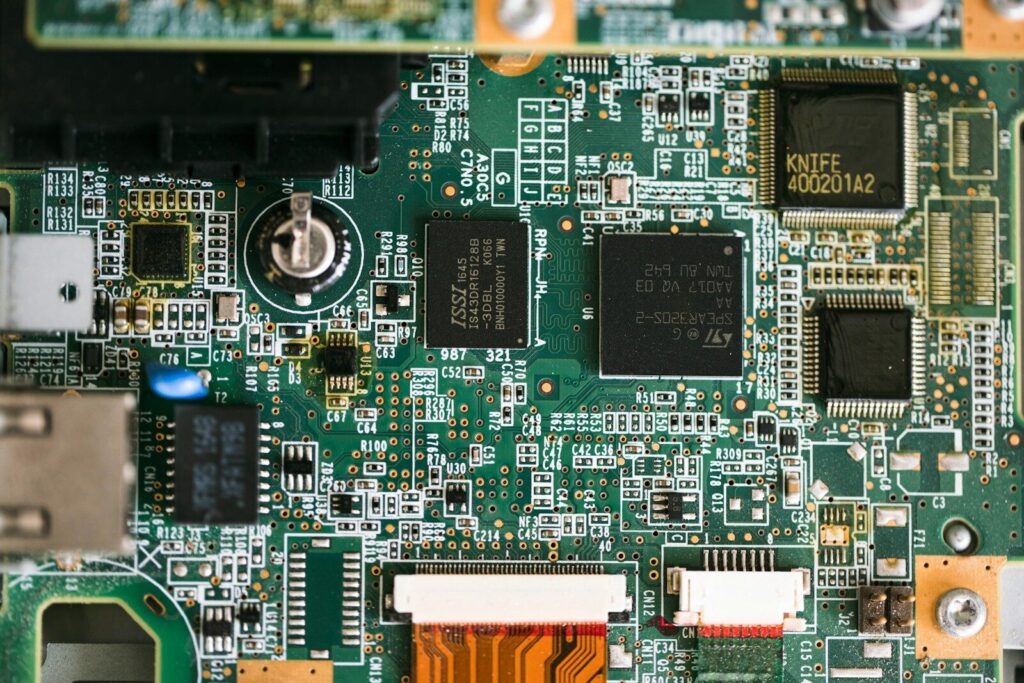
A printed circuit board is an insulating substrate laminated with copper, etched into signal paths, and drilled so components can be mounted and connected. It provides the physical frame and the electrical wiring of a circuit in a single part.
In operation, traces route current between the solder pads where components sit. The components themselves do the work of the circuit: resistors limit current, capacitors store charge, and transistors switch signals. Getting that arrangement right is the job of printed circuit board design, which turns a schematic into a physical layout and decides trace widths, spacing, layer count, and where each part lands on the board. The same board can carry power, analog signals, and high-speed digital traffic on separate layers, all without a single loose wire.
Components attach in one of two ways. Through-hole parts have wire leads that pass through drilled holes and are soldered on the opposite side. Surface-mount parts sit directly on pads and are soldered by reflow. Surface-mount technology now dominates because it packs more parts into less space and suits automated assembly lines.
Each method has trade-offs. Through-hole joints are mechanically strong, which helps with heavy parts and harsh environments, while surface-mount joints are smaller and better suited to high-volume production. Many real boards mix the two on one panel.
The four layers of a standard PCB
A finished board stacks four functional layers, though multilayer boards repeat the conductive and insulating layers many times.
| Layer | What it does | Common materials |
|---|---|---|
| Substrate | Insulating core that gives the board rigidity and strength | FR-4 fiberglass epoxy, polyimide, aluminum, ceramic |
| Copper | Conductive foil etched into traces and pads | Electrodeposited copper foil in standard weights |
| Solder mask | Insulating coating that protects traces and stops solder bridges during assembly | Epoxy-based liquid or dry film, most often green |
| Silkscreen | Printed labels marking part positions, polarity, and test points | Epoxy ink, usually white |
Common components on a PCB
The parts on a board vary by function, but most circuits draw from the same short list:
- Resistor: limits or regulates current flow.
- Capacitor: stores charge and releases it when the circuit needs it.
- Diode: lets current flow in one direction only.
- Transistor: amplifies signals or acts as an electronic switch.
- Inductor: stores energy in a magnetic field and filters current changes.
- Sensor: converts physical input such as motion, light, or heat into an electrical signal.
- Battery or connector: supplies power to the circuit.
- Switch: opens and closes the path of current.
What are printed circuit boards made of?
Most printed circuit boards start with FR-4, a fiberglass-reinforced epoxy laminate, bonded to copper foil that carries the circuit.
Material choice follows the application. Heat, signal frequency, flexibility, and cost all push the selection toward one base or another, and the printed circuit board material often defines the whole category of board. A buyer does not usually pick the laminate alone; the stackup comes out of the design’s thermal and frequency needs, and the fabricator then confirms it can build that stack reliably.
| Printed circuit board material | Key traits | Typical applications |
|---|---|---|
| FR-4 | Strong, low cost, good electrical insulation | Consumer electronics, industrial controls |
| Polyimide | Flexible and stable at high temperatures | Flex and rigid-flex circuits, aerospace, wearables |
| Metal core, usually aluminum | Draws heat away from components | LED drivers, power supplies, automotive lighting |
| Ceramic | Excellent heat and chemical resistance | High-power modules, medical and automotive boards |
| High-frequency laminates | Stable electrical behavior at high speeds | RF, telecom, and radar equipment |
What are the main types of PCBs?
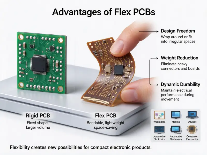
PCBs are grouped by substrate flexibility and by the number of conductive layers they carry. The flexibility split produces three families: rigid, flexible, and rigid-flex.
| Type | Structure | Common uses |
|---|---|---|
| Rigid | Solid FR-4 or metal substrate that cannot bend | Computers, appliances, industrial equipment |
| Flexible | Bendable polyimide film | Phones, cameras, medical devices, wearables |
| Rigid-flex | Rigid sections joined by flexible layers | Aerospace, defense, compact high-reliability devices |
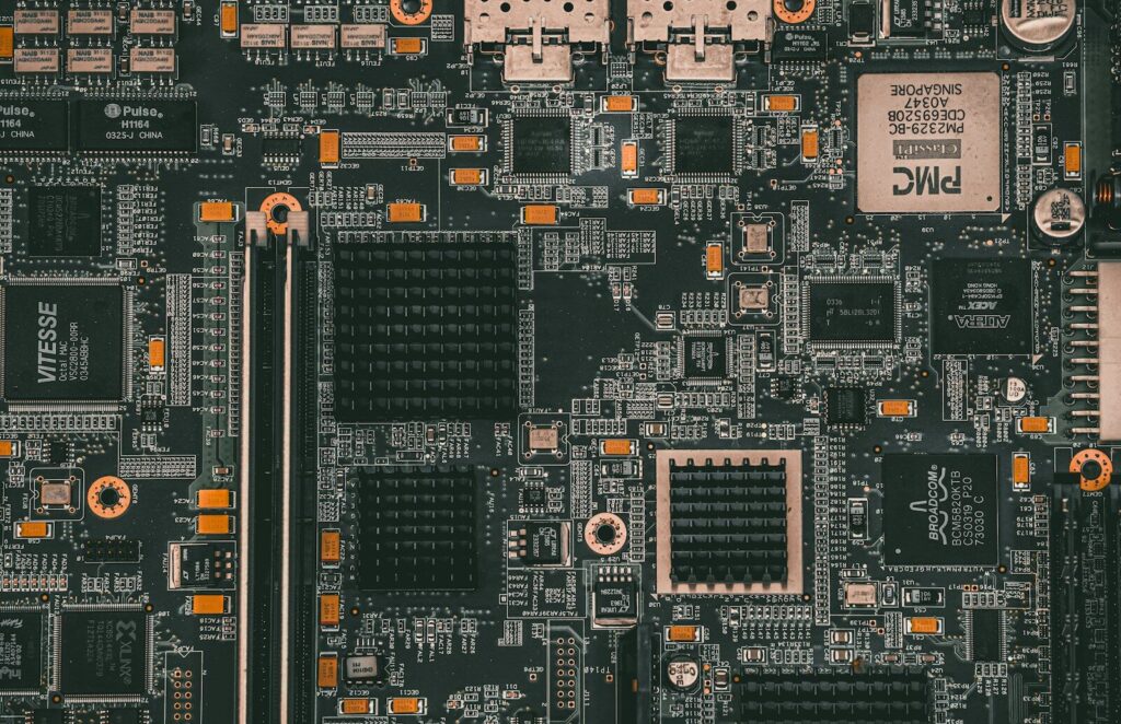
Layer count adds a second axis. Single-sided boards carry copper on one face and suit simple products. Double-sided boards route circuits on both faces, which raises density without much extra cost. Multilayer boards stack four or more conductive layers separated by insulation and serve complex hardware such as server boards and automotive control units. More layers mean more routing space and better signal isolation, at the price of thickness and cost.
Special categories cut across both axes. High-density interconnect (HDI) boards use finer lines and microvias to fit more parts per area, which suits phones and compact modules. High-frequency boards use low-loss laminates for RF work. Metal-core and ceramic boards trade cost for thermal performance. Buyers rarely need to memorize the categories; the application and the operating environment usually determine the right choice, and a fabricator can match material and process to it.
PCB vs. PCBA: What is the difference?
A PCB is the bare, unpopulated board. A PCBA, short for printed circuit board assembly, is that same board after components have been soldered in place and the finished circuit has passed inspection.
| Aspect | PCB | PCBA |
|---|---|---|
| State | Bare board with traces only | Fully populated and tested |
| Components | None | Resistors, ICs, connectors soldered on |
| Function | Cannot operate on its own | Performs its designed electronic function |
| Quoting basis | Size, layer count, base material | Adds component cost and assembly labor |
The distinction matters when you request quotes, because confusing the two is a common and expensive mistake and the two prices can differ by an order of magnitude. Buyers who lack surface-mount lines often order turnkey PCB assembly instead, so one supplier sources the parts, assembles the boards, and runs functional tests. That removes the freight, handling, and finger-pointing that appear when a bare board ships between two different houses. When you do compare quotes, ask which stage the price covers. A bare-board quote includes fabrication only, while a full assembly quote must also account for component sourcing, stencil setup, and test time.
How are PCBs manufactured?
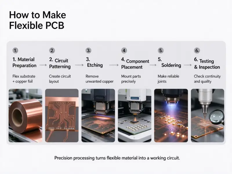
PCB manufacturing follows a fixed sequence, from transferring the circuit pattern onto copper to final electrical tests. Exact recipes vary between fabricators, but the sequence itself is standard across the industry.
Each step depends on the one before it, which is why fabricators hold tight process controls and why a design that ignores manufacturing rules creates yield problems downstream.
- Pattern transfer: the circuit image is printed onto copper-clad laminate with a photoresist.
- Etching: unwanted copper is dissolved away, leaving the traces and pads.
- Lamination: for multilayer boards, cores and prepreg are fused together under heat and pressure.
- Drilling: holes are cut for through-hole leads and vias that connect the layers.
- Plating: copper is deposited inside the holes to make the layer-to-layer connection conductive.
- Solder mask and silkscreen: the protective coating is applied, then the identification legends.
- Surface finish: exposed pads receive a protective metal coating to prevent oxidation.
- Electrical test and inspection: automated testing verifies that every connection matches the design.
A bare board that passes these steps becomes a PCB. Add component placement and reflow soldering, and it becomes a PCBA. Fabricators package finished boards in moisture-barrier bags so they arrive at the assembly line ready for processing.
What does PCB mean in other contexts?
Outside the electronics industry, PCB usually refers to polychlorinated biphenyls, a class of industrial chemicals. In online slang, the same letters form an abbreviation with crude meanings, so the surrounding context decides the meaning.
What does PCB slang mean?
In texting and on social platforms, PCB appears as a shorthand abbreviation, and in both English and Spanish-speaking online communities it often carries a vulgar meaning. Some users type the letters deliberately to slip past content filters. For business readers the rule is simple: in datasheets, invoices, and sourcing documents, PCB means the board, and slang usage is background noise worth recognizing but not acting on.
What does PCB mean in healthcare?
In healthcare and environmental reports, PCB stands for polychlorinated biphenyls. These man-made organic chemicals were prized for their chemical stability and used widely in electrical equipment until production bans took hold in the late 1970s. They persist in soil and water, accumulate in the food chain, and exposure is linked to a range of health effects.
The US Environmental Protection Agency maintains an overview of polychlorinated biphenyls and their health effects that serves as the standard reference when the term appears in medical or environmental documents. The two meanings never overlap in practice: a circuit board order and a toxicology report will never be about the same PCB. Some facility and safety audits still surface the chemical meaning decades after the bans, because older equipment can contain the substances.
FAQ
Is a motherboard the same as a PCB?
No. A motherboard is one specific, large multilayer PCB that carries a computer’s main interconnections and sockets. Every PCB is a circuit board, but only the central board of a computer system is a motherboard. Motor drives, charger circuits, and sensor boards are all PCBs too, and most of them look nothing like a motherboard.
Why are most PCBs green?
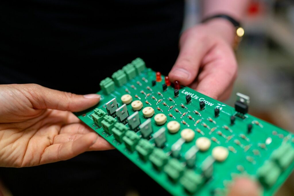
The green comes from the solder mask, not the board itself. Early mask formulations used pigments that cured reliably and offered good contrast for visual inspection, and the color became the industry’s visual signature. Red, blue, black, and white masks are now common, and the color has no effect on electrical performance. If a specific color matters for inspection or branding, state it in the fabrication notes rather than assuming green by default.
What does FR-4 mean on a PCB?
FR stands for flame retardant, and 4 is the grade designation in the material standard. FR-4 is a glass-reinforced epoxy laminate that balances strength, insulation, and cost, which is why it remains the default substrate for rigid printed circuit boards. Material datasheets list its glass transition temperature, and designs that run hot may call for a higher-grade laminate instead.