Most people meet a PCB from the component side, where it looks like a green slab holding a chip and a few capacitors. That view hides the answer to how a PCB is made. A printed circuit board is a short stack of ordinary materials, arranged so a design file becomes copper that carries current, insulation that keeps currents apart, and a surface that can be soldered. Order custom PCB manufacturing and what comes back is a physical object with material limits attached, not a drawing.
A PCB is made by taking an insulating core clad with copper, keeping copper only where the circuit needs it, and then adding the layers that protect and label the board. The copper pattern comes from a design file. The holes that link layers are drilled and plated so their walls conduct. The finish on the pads decides how well components solder. Everything else on the board exists to hold that copper, insulate it, or identify it.
Materials come first, because they explain most of the differences between two boards that look alike.
What a PCB is made of, layer by layer
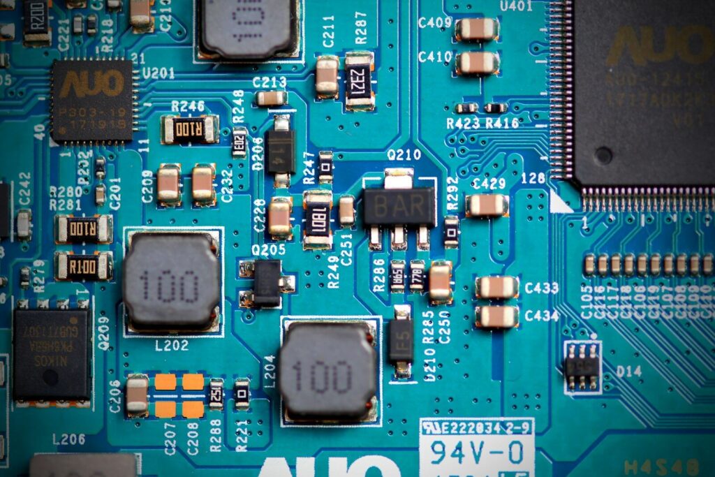
Four materials do nearly all the work: a base laminate that insulates and carries the structure, copper that carries current, a solder mask that covers the copper you do not want soldered, and a silkscreen that labels the board.
The stack builds from the bottom up: laminate in the middle, copper bonded to one or both faces, solder mask over the copper, silkscreen last. Almost all the thickness comes from the laminate and the foil, so every other layer is specified in microns.
The base laminate: the insulating core
The base is a reinforcement soaked in resin, and standard FR-4 uses woven glass cloth in epoxy. Glass transition temperature decides where the resin softens and the board starts to move under heat, with standard FR-4 near 130 to 140 C and high-Tg grades reaching 170 C and above for boards that run hot or see several reflow cycles. Laminate and prepreg grades are catalogued in IPC-4101E, which lists base materials for rigid and multilayer printed boards so grades can be compared by reinforcement, resin system, and glass transition temperature.
Copper: the layer that becomes the circuit
Copper is ordered by weight, not thickness: one ounce per square foot is roughly 35 microns, half an ounce about 18, two ounces about 70. Heavier copper carries more current and spreads heat better, but it etches more slowly and sets a floor under how fine traces can be.
Solder mask and silkscreen
Solder mask is a photoimageable epoxy ink cured over the copper. It stops solder bridging between pads, blocks oxidation, and narrows exposed copper to the pads that need solder. Green is common, but colour is cosmetic. Silkscreen, or the legend, is cured ink printed over the mask with reference designators, polarity marks, and board revision.
| Layer | Typical material | What it does |
|---|---|---|
| Base laminate | Woven glass cloth in epoxy resin (FR-4) | Insulates the copper layers, carries the structure |
| Copper | Foil bonded to the core, 0.5 to 2 oz per square foot | Carries current, forms traces and pads |
| Solder mask | Photoimageable epoxy ink | Keeps solder off unwanted copper, blocks oxidation |
| Silkscreen | Cured epoxy ink | Labels components, polarity, board identity |
How the copper pattern becomes a circuit
Most boards are built by subtraction. Copper is removed everywhere the circuit does not need it, holes are drilled and their walls made conductive, and the board is then protected and tested. Some advanced processes build copper up instead of etching it back, but the objective never changes: leave conductive metal only where the design asks for it.
Subtraction works the same way on every layer. A light-sensitive resist goes onto the copper, is exposed to ultraviolet light through a film, and is developed so only the areas to be removed stay soluble. Etchant dissolves that copper, the resist is stripped, and the layer is inspected before it is bonded to anything else, because a defect inside a pressed stack cannot be repaired later.
| Stage | What changes on the board |
|---|---|
| Engineering review and panelization | Files become shop data, boards are arranged on one panel |
| Image transfer | A resist pattern is developed onto the copper |
| Etching | Unwanted copper is dissolved; traces remain |
| Lamination | Cores, prepreg, and foil are pressed into one board |
| Drilling and plating | Holes appear and their walls conduct |
| Outer layer forming | The outer copper pattern is completed |
| Solder mask, legend, finish | Copper is covered, labelled, and made solderable |
| Profiling and electrical test | Boards are cut free and checked against the netlist |
Single-sided, double-sided, and multilayer
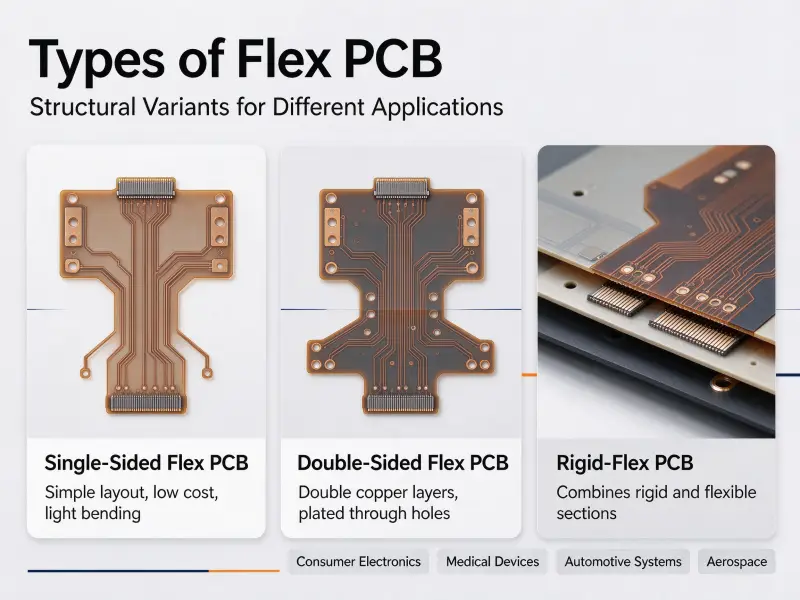
A single-sided board has one copper layer and needs no plated connections. A double-sided board adds a second layer, tied together with plated through-holes. On a multilayer board the imaging and lamination pair repeats for each layer pair, and every repeat adds another chance for layers to shift before the press closes. That repetition, not board area, drives the price gap between a two-layer and an eight-layer design of the same size.
When etching is not the whole story
Semi-additive processes plate copper onto a thin seed layer instead of etching a full foil back down, because trace widths eventually get too fine for a wet etchant to hold under the resist. High-density interconnect boards use laser-drilled microvias and sequential lamination, pressing layer pairs one round at a time. Printed electronics skip foil entirely and print conductive ink on flexible film, which suits antennas and low-power sensors but gives up copper’s conductivity.
Types of PCB and what each one changes
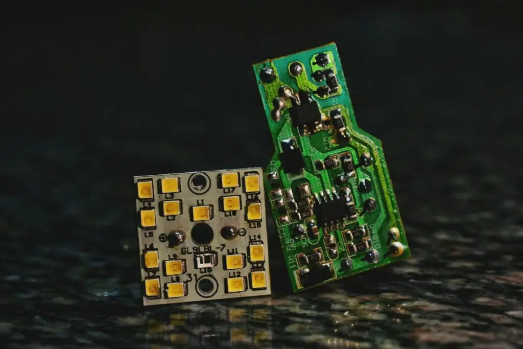
Board type does not change how a board is made in principle. It changes the material, the number of layers, and how small the geometry has to be, and those three things set the process, the tolerance, and the price.
| Type | Made from | Typical use | What it changes |
|---|---|---|---|
| Single-sided | Paper or composite laminate, one copper layer | Power supplies, simple controls | Cheapest, no layer connections |
| Double-sided | FR-4 with two copper layers | Consumer devices, LED boards | Adds plated through-holes |
| Multilayer | FR-4 cores bonded with prepreg | Computers, industrial controls | Repeats lamination, tighter registration |
| Rigid | FR-4 | Most electronics | Standard build flow |
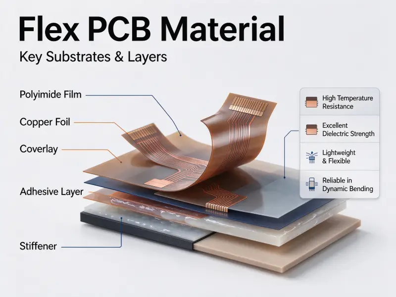
| Flexible | Polyimide with a coverlay | Wearables, cameras, tight enclosures | Bends and folds |
| Rigid-flex | FR-4 joined to polyimide sections | Medical, aerospace, dense assemblies | Two flows in one stack-up |
| HDI | FR-4 or better with laser microvias | Phones, tablets, dense modules | Sequential lamination, microvias |
| Metal core | Aluminium or copper base, thin dielectric | LED lighting, power electronics | Heat escapes through the base |
| Ceramic | Alumina or aluminium nitride | RF, high temperature, sensors | Different drilling and finishing |
The useful question is not which type sounds advanced but which type the product needs. A wearable needs flexible material because it bends, an LED driver needs a metal core because it runs hot, and a board with a few dozen parts usually needs nothing more exotic than double-sided FR-4.
Do PCB boards have gold?
Yes, but the gold is nothing like a coating of solid metal. On most boards it is a layer a fraction of a micron thick sitting on top of nickel, present only on the pads, and it dissolves into the solder joint during reflow. It is there to protect the nickel from oxidising before assembly.
Immersion gold over nickel
Immersion gold, known as ENIG, is a two-layer finish. Electroless nickel goes down first at 3 to 6 microns and acts as both the copper diffusion barrier and the surface the solder bonds to. Immersion gold follows at 0.05 to 0.1 micron, and its only job is to keep that nickel clean until assembly.
Both deposits are chemical rather than electroplated, so the finish covers isolated pads evenly and stays flat. That flatness is why ENIG is common on boards with ball grid arrays and fine-pitch parts, where a domed pad tilts a component or traps flux.
The process has limits. Gold that is too thin leaves nickel exposed during storage. Gold that is too thick wastes money on a metal that ends up inside the joint and can make it brittle. Poor bath control corrodes the nickel instead of plating it cleanly, the failure the industry calls black pad.
Hard gold: when wear resistance matters
Electroplated gold is used where the board itself acts as a connector: card edge fingers, spring contacts, and pads that slide or are inserted repeatedly. Hard gold is measured in whole microns and is specified for wear, not for soldering.
| Finish | Flatness and cost | Where it is used |
|---|---|---|
| HASL | Lowest cost, uneven surface | General purpose, through-hole-heavy boards |
| OSP | Low cost, very flat | Short-life boards, fine-pitch work |
| Immersion silver | Moderate cost, flat | Fine pitch where gold is not required |
| Immersion tin | Moderate cost, flat | Press-fit and some fine-pitch assembly |
| ENIG | Higher cost, very flat | Fine pitch, ball grid arrays, long shelf life |
| Hard gold | Highest cost, plated thick | Edge connectors and contacts that wear |
What is the cheapest PCB material?
For a simple single-sided board with few components and little heat, the cheapest option is a paper-based phenolic laminate such as FR-1 or FR-2. CEM-1 sits between paper and glass. Standard FR-4 costs more than either. The moment a design needs more than one layer, repeated reflow, or real reliability, the cheapest material becomes the expensive mistake.
The low-cost ladder
FR-1 and FR-2 use a paper core with phenolic resin, sit at the bottom of the price ladder, and can be punched rather than drilled. CEM-1 uses epoxy resin over a paper core with woven glass surfaces, so it tolerates heat better than the paper grades while staying below FR-4. CEM-3 moves the core to non-woven glass and supports double-sided work. Above that come standard FR-4, high-Tg FR-4, then specialist materials such as polyimide, PTFE, and ceramic. The order is stable, but the size of the gaps is not, because laminate price depends on thickness, panel utilization, and order volume as much as on grade.
When cheap material backfires
The trade-offs are not subtle, and they arrive in a predictable order once a product stops being simple.
- Reflow. Paper cores carry lower continuous-use temperature ratings than glass-reinforced grades, so a board that sees reflow more than once can delaminate or warp.
- Moisture. Paper absorbs water faster than glass cloth, so a board used in humid air can swell and shift trace geometry.
- Structure. Paper laminates are limited to single-sided work with no plated through-holes, so multilayer designs rule them out.
- Electrical. Dielectric constant and loss vary more between batches than on consistent FR-4, so impedance-controlled designs need material that behaves the same way every time.
- Compliance. The flame rating has to satisfy the standard that applies to the end product, and the wrong flammability class can block a certification.
| Material | Layers supported | Typical products | Main limit |
|---|---|---|---|
| FR-1 and FR-2 | Single-sided | Remotes, calculators, simple toys | Delaminates in repeated reflow, absorbs moisture |
| CEM-1 | Single-sided | Power adapters, LED drivers | No plated holes or multilayer |
| CEM-3 | Double-sided | Simple control boards | Not consistent enough for impedance control |
| Standard FR-4 | Single to multilayer | Most electronics | Costs more than composite laminates |
| High-Tg FR-4 and above | Multilayer | Automotive, networking, aerospace | Material cost rises sharply |
Material is only one line in a quotation. Layer count, copper weight, minimum trace and spacing, surface finish, tolerance, quantity, and lead time all move the PCB price, which is why two factories can return different numbers for the same file and both be right.
From bare board to working circuit: where components come in
Fabrication ends with a bare board. Assembly is what turns it into a circuit that does something, and it is a separate process with its own equipment, materials, and inspection. A board that passes bare-board testing can still fail once parts are on it.
Solder paste, placement, and reflow
A stainless stencil prints solder paste onto the pads, a placement machine sets surface-mount parts in position, and the board travels through a reflow oven where the paste melts, wets the pads, and forms the joints. Through-hole parts take a different path: leads are inserted and the board passes over a wave of molten solder.
Testing a finished assembly
Inspection runs in layers. Automated optical inspection compares the board with the placement file to catch missing, offset, or rotated parts. In-circuit testing or flying probe checks continuity and resistance net by net. Functional testing runs the board the way the product will run it.
A bare board is a PCB. The same board with components soldered on it is a PCBA, and the two are usually built by different suppliers under different standards. Assembly houses typically buy parts through B2B electronic components sourcing, because component availability moves a schedule far more than the bare board does.
FAQ
Can a PCB be made without copper?
Yes, for circuits that do not need much current. Printed electronics deposit conductive ink, often silver-based, onto flexible film and build traces by printing rather than etching. The result is thinner and lighter than foil on laminate, but its resistance is far higher, so it suits antennas, membrane keypads, and low-power sensors.
Why do PCBs have so many small holes?
They serve three purposes and only one is electrical. Vias connect copper on different layers, and a cluster of small vias under a power device is deliberate, moving heat into a copper plane instead of letting it build up locally. Component holes hold the leads of through-hole parts, and the rest are mechanical: tooling holes that align the panel and mounting holes that take screws in the finished product.
Are homemade PCBs as reliable as factory-made boards?
Not in the sense that matters for a product that ships. Hand etching leaves a wider tolerance on trace width, cannot produce plated through-holes, has no registered solder mask, has no controlled copper thickness, and ends without an electrical test against the netlist. For a one-off prototype that is a fair trade, but anything beyond two layers is out of reach at the bench.