Most of what a bare board costs, and how long it lasts, is settled before anything reaches the production line. The laminate grade, copper weight, mask, and finish are chosen in a review meeting and written into a drawing. Buyers who know what each layer does can compare custom PCB manufacturing quotes on equal terms.
A PCB board is made of laminated layers rather than one solid material. The base is a dielectric substrate, usually woven fiberglass cloth bonded with flame-retardant epoxy resin and known as FR-4. Copper foil is bonded to one or both sides and etched into traces, pads, and planes. Above the copper, a solder mask blocks solder bridges and oxidation, and a silkscreen prints reference marks. Exposed pads then get a surface finish that keeps the copper solderable, such as hot air solder leveling or electroless nickel immersion gold. Multilayer and flexible boards add prepreg, coverlay, and plated vias to the same set.
Read the stack from the outside in, and a material specification starts to make sense.
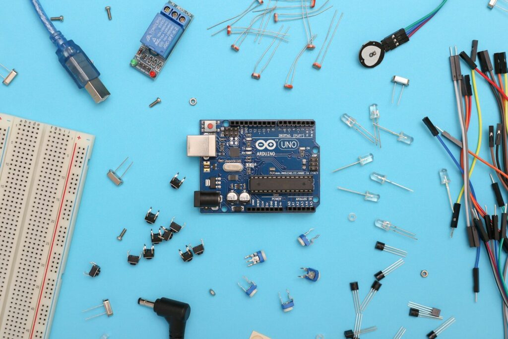
The layer stack of a PCB board, layer by layer
A finished rigid board is five materials pressed into one: a substrate core, copper on one or both sides, a solder mask, a silkscreen legend, and a surface finish over the exposed copper. Multilayer boards repeat the substrate and copper layers, bonded with prepreg.
Each layer settles onto the one below it, and reading that sequence is the first step in PCB learning.
| Layer | Typical material | What it does | Cost position |
|---|---|---|---|
| Silkscreen | Epoxy ink, white by default | Designators and polarity marks | Low |
| Solder mask | Photoimageable polymer | Insulation blocks bridges | Low to moderate |
| Copper foil | Electrodeposited or rolled copper | Carries signal and power | Rises with copper weight |
| Substrate core | Woven glass cloth in epoxy | Support, insulation, dielectric | Largest material line |
| Surface finish | Solder, nickel and gold, silver, organics | Keeps copper solderable | Rises with gold content |
| Prepreg | Resin-impregnated glass cloth | Bonds cores, sets spacing | Moderate |
Five material layers from top to bottom
Silkscreen is ink and only sits where solder will not go. Solder mask decides which copper may be soldered and which is sealed. Copper carries the current, and surface finish exists because oxidized copper does not wet solder.
How rigid, flex, and rigid-flex stacks differ
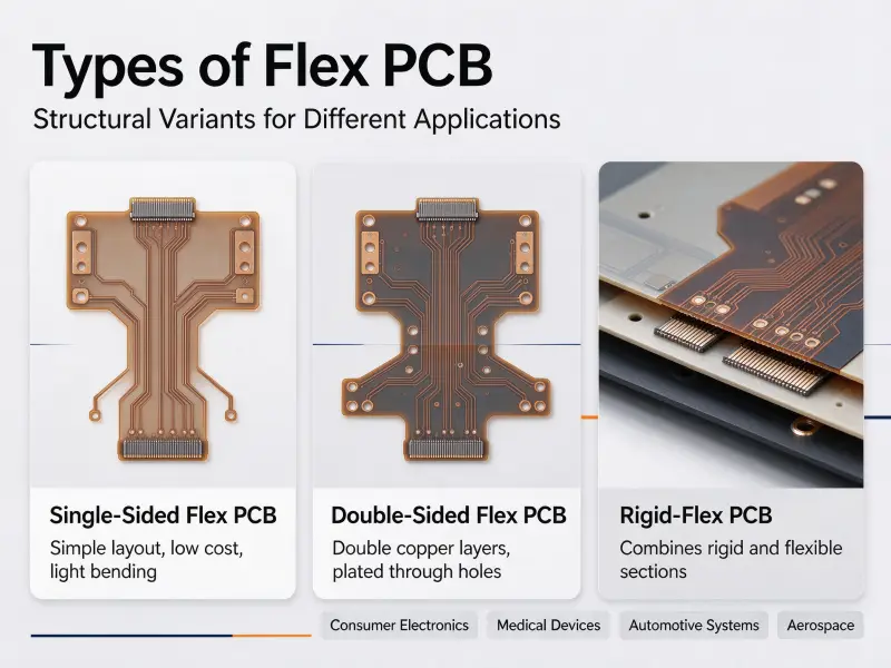
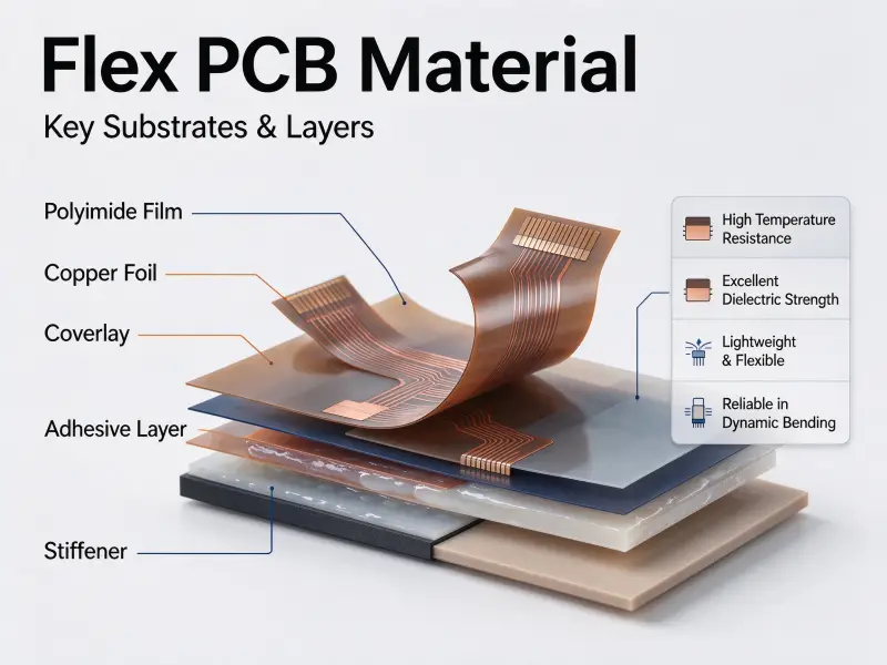
A flexible board swaps the rigid core for polyimide film and the solder mask for a coverlay. Stiffeners sit where connectors would stress the film, and rigid-flex boards laminate flex sections into rigid islands in one build, so the types of PCB differ in material rather than layer count alone.
What a PCB board is not made of
It is not a plastic sheet, because the strength comes from glass cloth rather than resin alone, nor pure glass, since the glass arrives as woven fabric soaked in resin. It is not metal: copper sits only on the conductive layer, and aluminum only as the base plate of a metal core board.
Substrate materials: FR-4 and its alternatives
The substrate is the insulating core that gives the board its strength and its dielectric properties. FR-4 covers most rigid boards. Where a design needs flexibility, higher heat resistance, tighter dielectric control, or better heat spreading, the core changes to a composite epoxy material, polyimide, a PTFE-class low-loss laminate, a metal core, or a ceramic plate.
Its glass transition temperature decides how much heat the resin survives, its dielectric constant decides signal velocity, and its thickness with the copper weight sets the finished board thickness.
FR-4 and Tg grades
FR-4 is a family, not a single product. Suppliers certify grades against IPC-4101, the base materials specification for rigid and multilayer boards, which sorts them by reinforcement, resin system, and glass transition temperature. Standard grades sit near 130 to 140 degrees Celsius, and high Tg grades at 170 and above, with lead-free reflow and thick stacks pushing a design higher. A dielectric constant of roughly 4.2 to 4.7 with a loss tangent near 0.02 is why FR-4 suits ordinary digital work and loses its advantage as frequency climbs.
CEM-1 and CEM-3 for cost-sensitive boards
CEM-1 uses a cellulose paper core with woven glass surfaces, and CEM-3 uses non-woven glass throughout. Both reach a glass transition temperature in the 110 to 130 degree range and cost less than FR-4, but the paper core cannot take reliable plated through-holes, so CEM-1 stays in single-sided work.
Polyimide and PTFE for flexible and high-frequency designs
Polyimide is the standard flex substrate, tolerating higher soldering temperatures than FR-4 and surviving bend cycles in camera modules. PTFE and the low-loss laminates built around it serve radio frequency work, where a dielectric constant nearer 2.2 keeps signal loss predictable.
Metal-core and ceramic substrates
An aluminum-backed metal core PCB spreads heat from high-power LEDs across the board instead of concentrating it under the part. Ceramic substrates, typically alumina or aluminum nitride, add high thermal conductivity and expansion close to silicon.
What is the cheapest PCB material?
Paper-based laminates are the cheapest rigid substrates on the market, and CEM-1 is the step up from them.
| Substrate | Reinforcement and resin | Typical Tg | Flame rating | Typical use |
|---|---|---|---|---|
| FR-2 | Cotton paper, phenolic | 105 Celsius | Horizontal burn | Single-sided consumer boards |
| FR-1 | Paper, modified phenolic | 105 to 110 Celsius | Vertical burn, flame-retardant grades | Boards needing better insulation |
| CEM-1 | Paper core, glass surfaces | 110 to 120 Celsius | Vertical burn | Power supplies and LED drivers |
| CEM-3 | Non-woven glass, epoxy | 120 to 130 Celsius | Vertical burn | Cost-sensitive double-sided boards |
| FR-4 | Woven glass cloth, epoxy | 130 to 180 Celsius by grade | Vertical burn | Rigid and multilayer work |
Cheap holds only inside an envelope: paper cores cannot take plated through-holes, low glass transition temperatures make lead-free reflow difficult, moisture absorption runs several times that of FR-4, and a horizontal burn rating can fail appliance safety tests.
Copper: the layer that carries the current
Copper foil is the conductor. It is laminated to the substrate, then imaged and etched into traces, pads, and planes, while plated holes connect the layers vertically. Copper thickness, quoted in ounces per square foot, sets current capacity, thermal spreading, and board weight.
Copper weight and what it decides
Half an ounce per square foot works out to roughly 17.5 micrometers, one ounce to about 35, and two ounces to about 70. Heavier copper carries more current at the same trace width and spreads heat, but it also slows etching, so fine line work gets harder.
ED copper versus rolled annealed copper
Electrodeposited copper is grown onto a rotating drum, leaving one matte side and one smooth side with better line definition, so it suits rigid boards. Rolled annealed copper is milled from an ingot, and its grain structure tolerates repeated flexing.
Traces, planes, and vias inside the stack
Signal layers carry traces, while plane layers are solid copper for power, ground, and reference. Vias join layers as through, blind, or buried holes, limited by the aspect ratio a process can plate reliably, and this is where the working density of a PCB circuit is decided.
Solder mask, silkscreen, and surface finish
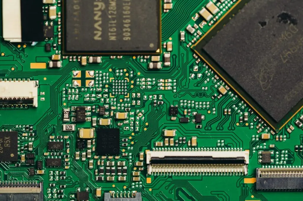
The solder mask is a thin polymer coating that covers the copper you do not want soldered, the silkscreen prints the legend on top of the mask, and the surface finish is the coating applied to exposed copper so it still wets solder after storage.
Solder mask and why color is mostly cosmetic
Liquid photoimageable solder mask opens over pads and stays over everything else. It prevents solder bridges between fine-pitch pads, protects copper from oxidation and handling damage, and gives automated optical inspection the contrast it needs. Green is the default only because of long process experience, so the color is largely cosmetic.
Silkscreen and the legend layer
Silkscreen carries reference designators, polarity marks, pin one indicators, and board revision. It prints onto the cured mask and must stay clear of pads, because ink on a pad interferes with wetting.
Surface finish options and where each one fits
| Finish | What it is | Strength | Limitation |
|---|---|---|---|
| Hot air solder leveling | Solder leveled with hot air | Robust, inexpensive, and rework-friendly | Uneven, poor for fine pitch |
| Electroless nickel immersion gold | Nickel barrier with a thin gold cap | Flat, long shelf life | Higher cost, tight process control |
| Immersion silver | Thin silver layer over copper | Flat, suited to RF | Tarnishes, handling sensitive |
| Organic solderability preservative | Organic film over copper | Very low cost, flat | Short shelf life |
| Hard gold | Thick gold over nickel on contacts | Resists wear when mated | Not a solderable finish |
Do PCB boards have gold?
Sometimes, and very little of it. Gold appears in electroless nickel immersion gold, where a thin cap protects a nickel barrier; the finish specification published by IPC places nickel at roughly 3 to 6 micrometers with gold around 0.05 to 0.1 micrometers. It also appears as hard gold on edge connectors and keypads, where the layer is thicker because it must survive repeated mating.
How material choices drive PCB price
Material grade is one of the few cost drivers a buyer controls directly. Layer count, copper weight, laminate grade, surface finish, and fabrication tolerance all move the price, and most of them move it through extra process steps and yield loss rather than raw material alone.
The cost drivers behind a PCB quote
- Layer count, since each added pair brings another lamination and drilling pass.
- Substrate grade, because a high Tg or low-loss laminate may need a longer cycle.
- Copper weight, since heavier foil increases etching time and scrap.
- Surface finish and plated area, driven by gold content and exposed copper.
- Feature size, including narrow line and spacing, and controlled impedance.
- Board size and panel utilization, which decide units per panel.
- Quantity, because setup costs spread over a larger order.
- Testing and acceptance class, since electrical tests and strict criteria add steps.
Where cheaper materials cost more
A paper-based core that fails under lead-free reflow takes the whole lot with it. Moisture absorption several times higher than FR-4 can drive delamination and insulation failures, and a flame rating that misses the target market’s appliance standard can stop a shipment at the border.
Matching materials to the application
Material selection is requirements matching. The electrical environment sets the dielectric, the thermal and mechanical environment sets the resin and reinforcement, and the target market sets the compliance paperwork.
Electrical requirements: Dk, Df, and impedance control
The dielectric constant decides signal velocity and the trace width needed for a target impedance, and the loss tangent decides how much signal turns into heat. Matching the stack to the frequency range matters more in PCB board design than buying the most expensive laminate.
Thermal and mechanical requirements: Tg, Td, CTE, and moisture absorption
Glass transition temperature marks where the resin softens, and working above it invites expansion, drill smear, and delamination. Z-axis expansion mismatched against the copper barrel is the classic cause of barrel cracks after thermal cycling.
Compliance: flame rating, restricted substances, and acceptance class
A vertical burn rating is often a market entry requirement for appliances. Restricted substance rules removed lead from the process, and acceptance class sets how much cosmetic and structural deviation is tolerated.
| Application | Typical substrate | Typical finish | Dominant driver |
|---|---|---|---|
| Single-sided consumer control boards | FR-2 or CEM-1 | Hot air solder leveling | Cost per unit |
| Industrial control and power | FR-4, standard or high Tg | Solder leveling or ENIG | Thermal cycling |
| Automotive electronics | High Tg FR-4 | ENIG, or immersion silver | Temperature and service life |
| RF and microwave | PTFE-class low-loss laminate | ENIG, or immersion silver | Dielectric stability |
| LED lighting and power modules | Aluminum metal core | Solder leveling or ENIG | Heat spreading |
| Cameras, wearables, moving joints | Polyimide flex or rigid-flex | ENIG with hard gold on contacts | Bend cycling |
How to specify PCB materials in a quote request
A material specification only works if it travels with the files. The stack-up drawing, the laminate callout, and the finish requirement belong with the fabrication and drill data.
The material items a quote needs
- Layer count and the full stack-up sequence.
- Laminate family and glass transition temperature grade.
- Copper weight for each layer.
- Finished board thickness and its tolerance.
- Surface finish, named and referenced to the relevant standard.
- Solder mask color and coverage.
- Minimum line width and spacing, or the impedance target for controlled nets.
- Acceptance class and any certification the end customer requires.
- Quantity, delivery format, and panel preference, if any.
Documents that remove ambiguity
Fabrication data in Gerber or ODB++ format, the drill file, a stack-up drawing, an impedance table, and the laminate and finish callouts belong with the drawing. The bill of materials matters too, because the PCB components on it determine the pad geometry, and a silent laminate change between lots is a common cause of hard-to-trace field failures.
FAQ
Are halogen-free laminates required for RoHS compliance?
No. Restricted substance rules cover lead, mercury, cadmium, hexavalent chromium, certain polybrominated flame retardants, and a short list of phthalates, and the brominated flame retardant used in FR-4 is not one of them. Halogen-free is a separate end customer requirement that costs more and shifts the process window.
Can one board use two different laminate grades in the same stack-up?
Yes, and hybrid stacks are common in high-speed work. One or two layers carrying the fastest signals may use a low-loss laminate while the rest stay on FR-4, and rigid-flex boards already mix polyimide cores with rigid FR-4 islands. The trade-off is process complexity, since the materials expand differently.
Does solder mask or silkscreen color affect electrical performance?
Not in any practical sense, because the color comes from pigment in the same polymer and its effect on the dielectric is negligible at conventional frequencies. Dark masks do reduce the contrast automated optical inspection relies on, which can hide a defect under the coating.