Anyone who has shopped for electronics manufacturing has hit the wall of acronyms. PCB, PCBA, SMT, BOM, DFM — the list goes on, and two of those abbreviations sit next to each other on almost every quote, spec sheet, and supplier intake form. PCB and PCBA look nearly identical at a glance, which is exactly why so many first-time buyers mix them up. The confusion is understandable, but it gets expensive fast when a purchase order asks for the wrong item or a prototype falls behind schedule because the two were never defined clearly.
A PCB is the blank board itself — layers of fiberglass and copper etched into conductive pathways, with nothing attached. A PCBA is that same board after resistors, integrated circuits, and connectors are mounted and soldered into place, so it can actually run a circuit. In short, one is the foundation and the other is the finished, working assembly built on top of it. Teams that need both stages often start with a partner for custom PCB manufacturing and then move straight into assembly under one roof, which removes a handoff and keeps tolerances consistent.
The sections below break down how each is built, where they split apart, and what that means when you brief a supplier or place an order.

What is a printed circuit board (PCB)?
A printed circuit board (PCB) is the physical platform — an insulating base laminated with patterned copper that routes electricity between fixed points. On its own, it carries no active parts and does nothing until components are added.
A bare board is easier to understand once you look at what it is made of. The board is a stack of materials chosen for electrical isolation, mechanical strength, and thermal behavior. Most commercial boards use an FR-4 fiberglass substrate, but the family is far wider than that single material, and the choice drives cost, frequency performance, and reliability.
Substrate and copper stack
The substrate gives the board its shape and rigidity. Thin copper foil is bonded to one or both faces, then patterned through exposure, etching, and stripping so only the required traces remain. A trace is simply a flat copper wire frozen into the board. Vias — small plated holes — carry signals between layers when the design uses more than two copper planes. The result is a passive network of connections with no intelligence of its own.
Common board constructions
Not every board looks the same, and the construction you pick changes how it behaves in the field.
| Construction | Core trait | Typical use |
| Rigid PCB | Fixed shape, cannot bend | Power supplies, controllers, consumer electronics |
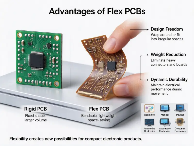
| Flexible PCB (FPC) | Bends and folds | Cameras, wearables, hinges in laptops |
| Metal core PCB (MCPCB) | Aluminum or copper base for heat | LED lighting, motor drives |
| Rigid-flex PCB | Rigid and flex zones joined | Aerospace, medical imaging |
| High-frequency PCB | Low-loss laminate | RF, radar, base stations |
Each variant starts from the same idea: a board that carries traces but no parts. The material and layer count are what separate a simple single-sided board from a dense, multilayer stack used in servers or telecom gear.
A board at this stage is sometimes called a bare board or blank PCB. It can be inspected, shipped, and stored on its own, which matters for supply chains that split manufacturing and assembly across sites or regions. That split is also where the PCB-versus-PCBA question stops being academic and starts affecting lead time and cost.
What is a PCBA, and how is it assembled?
A PCBA (printed circuit board assembly) is a PCB that has been populated with components and soldered, turning a passive board into a functioning electronic module. The “A” at the end stands for assembly, and that single letter is the entire difference between a part that sits on a shelf and a part that powers on. For teams new to the supply chain, the question of what a PCBA is usually comes down to one word: populated. A board with parts on it is a PCBA; a board without them is still just a PCB.
Assembly is a manufacturing process in its own right, with its own equipment, defects, and quality gates. A board that was perfect as a bare substrate can still fail here if a footprint is wrong or a component was placed a fraction of a millimeter off.
Surface-mount versus through-hole
Two mounting styles dominate modern assembly. Surface-mount technology (SMT) places tiny components directly onto pads on the board surface, which allows high density and fast automated placement. Through-hole technology (THT) pushes component leads through drilled holes and solders them on the far side, which is slower but gives stronger mechanical joints for connectors and heavy parts. Many boards use both: SMT for the dense logic, through-hole for things that get plugged in and pulled out.
The assembly workflow
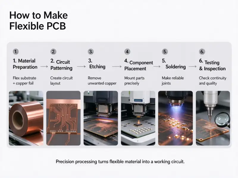
A typical turnkey line runs through a defined sequence:
- Solder paste is printed onto the pads through a stencil.
- A pick-and-place machine sets components onto the paste.
- The board passes through a reflow oven, melting the paste to form joints.
- Automated optical inspection checks placement and solder shape.
- Through-hole parts are wave or hand soldered where needed.
- The finished board is powered and functionally tested against its spec.
That last step is what makes a PCBA different from a pile of parts on a board. A bare PCB is judged on copper and material. A PCBA is judged on whether it works, which is why test coverage and yield matter as much as the components themselves. Buyers who want that whole chain handled together usually look for turnkey PCB assembly, where fabrication, sourcing, placement, and test sit inside one process rather than three separate vendors.

PCB vs PCBA: What Actually Changes
The difference is the presence of components. A PCB is an unpopulated board; a PCBA is a populated, tested, working board. Everything else — price, handling, testing, and how you specify it — flows from that single fact.
The table below shows where the two diverge so you can brief a supplier without ambiguity.
| Attribute | PCB | PCBA |
| Components mounted | No | Yes |
| Functional on its own | No | Yes |
| Primary input | Gerber, stack-up, material | BOM, centroid, Gerber |
| Main risk | Etch and material defects | Placement and solder defects |
| Testing | Continuity, impedance | ICT, functional test |
| Shipping form | Bulk, static-safe | Tray, reel, or ESD pack |
| Typical cost driver | Layer count, material | Component cost, placement density |
The distinction shows up in documents too. A PCB quote needs the board file and stack-up. A PCBA quote needs those plus a bill of materials, a placement file, and often a sourcing plan for long-lead parts. If you are still asking what the difference is between a PCB and a PCBA, start with the paperwork: the two are specified with different files, inspected to different standards, and shipped in different packaging. For the longer-form comparison, our page on PCB vs. PCBA walks through the split with more examples drawn from real builds.
A useful mental model: the PCB is the canvas, the PCBA is the painting. You cannot hang the canvas and expect it to show a picture, and you cannot paint without the canvas underneath. Both are real products with their own part numbers, their own inspection standards, and their own place in the supply chain.
When do you need a bare board versus a fully assembled one?
You need a bare PCB when the assembly happens somewhere else, and you need a PCBA when you want a board that is ready to drop into your product. The right choice depends on who is doing the soldering and why.
Prototype shops and research labs often buy bare boards so they can hand-place parts, swap values, and learn from failures without paying for a full assembly run each time. That flexibility has a cost in time and rework, but for early validation it is usually worth it. High-volume production moves the other way: once the design is locked, paying for a bare board and then staffing an in-house line rarely beats sending the whole job out.
Procurement strategy also plays a role. Some companies buy bare boards in bulk to hedge material lead times, then assemble closer to demand. Others consolidate everything with one supplier to cut logistics and keep traceability simple. Neither is wrong; they are different answers to the same question of where the value-added step should live.
The trap is ordering a PCB when you actually needed a PCBA, or vice versa, and discovering it only when the shipment arrives. A clear internal spec—board only, or board plus components—prevents that miss and keeps the production plan honest.
How printed circuit board design shapes assembly
A printed circuit board design decides how easy or painful the assembly step will be. Choices made in the layout tool echo all the way to test yield and field returns.
Design for manufacturing (DFM) is the discipline of laying out a board so it can actually be built at volume. Tight pads, missing fiducials, and components placed too close together all raise the chance of a misaligned placement or a cold joint. Footprints must match the real parts, not the generic symbol in the library, or the assembler spends hours resolving a mismatch that the designer could have caught in an afternoon.
Layer count and stack-up affect both the bare board and the assembly. A four-layer board gives cleaner power and signal separation than a two-layer one, but it costs more to fabricate and leaves less room for manual rework. Thermal design matters for assembly too: large copper pours can sink heat during reflow and cause uneven joints unless the profile is tuned.
Component selection ties design to sourcing. A part that is perfect on paper but unavailable for twelve weeks stalls the whole PCBA, no matter how good the layout is. Strong design teams work with their assembly partner early so the BOM reflects what can actually be bought, and so the board is drawn around parts that exist in quantity.

Choosing printed circuit board manufacturers for your build
Picking the right printed circuit board manufacturers is less about finding the lowest price and more about matching capability to your product. A shop that excels at simple two-layer boards may struggle with a ten-layer RF stack, and a house built for prototypes may not scale to your production volume without growing pains.
Start with the basics that apply to both stages. Certifications such as ISO 9001 and, for relevant markets, IPC and UL, tell you the line runs to a documented standard rather than by feel. Ask how they handle traceability: can they tell you which lot of laminate and which reel of parts went into a specific batch? For medical, automotive, or aerospace work, that paper trail is not optional.
Lead time and communication matter as much as the spec sheet. A supplier that quotes three weeks but slips to nine without warning costs you more than one that quotes five and holds it. Look for clear engineering review up front, where they flag DFM issues before fabrication instead of after.
This is also where consolidation pays off. Keeping fabrication and assembly with one partner means one accountable owner for the whole board, fewer finger-pointing loops when something fails, and a single source of quality data. Slpcba runs both stages — from bare board through populated, tested assembly — so the handoff that usually causes tolerance drift and schedule loss simply does not exist. For teams weighing build-versus-buy on the assembly side, our electronic manufacturing solutions cover prototyping, low-volume runs, and full turnkey production under one quality system.
If you are scoping a new board, the fastest path is to share the Gerbers and BOM with our team and get a real read on feasibility and cost before you commit tooling.
Common mistakes when ordering PCB and PCBA
Most failures in this category are avoidable, and they tend to repeat across first-time buyers. Watching for them saves both money and schedule.
The first mistake is treating PCB and PCBA as interchangeable in the request. A supplier cannot quote an assembly from a board file alone, and they cannot ship a working unit from a bare board. State clearly which one you need.
The second is sending an incomplete package. For a PCB, that means missing stack-up or impedance notes. For a PCBA, it means a BOM without manufacturer part numbers or a centroid file that does not match the layout. Each gap triggers a clarification round that pushes your slot further back.
The third is ignoring DFM feedback. When an assembler flags a footprint or a spacing issue, that note is a preview of a defect, not a formality. Closing it early is far cheaper than reworking a finished reel.
The fourth is separating fabrication and assembly without a plan for the handoff. Two vendors mean two sets of tolerances, two lead times, and two parties to coordinate when a board fails a test. For many builds, keeping both steps together removes an entire class of problems.
FAQ
Is PCBA just another word for PCB?
No. PCBA refers to a PCB that has already been populated with components and tested, while a PCB is the unpopulated board. Saying “PCBA” tells the supplier you expect a finished, working assembly, not a blank substrate.
Can I order a bare PCB and assemble it myself?
Yes, and many prototyping teams do exactly that to control iterations and cost. The trade-off is that you take on sourcing, placement, soldering, and testing yourself. For anything past a handful of boards, a turnkey assembly service usually wins on consistency and speed.
Which costs more, a PCB or a PCBA?
A PCBA almost always costs more because it includes the bare board plus components, placement, soldering, and testing. The board itself is often a small share of the total once active parts and labor are added, which is why component selection drives PCBA cost far more than layer count.