High-End Flexible PCB (FPC) Manufacturing for Foldable Devices
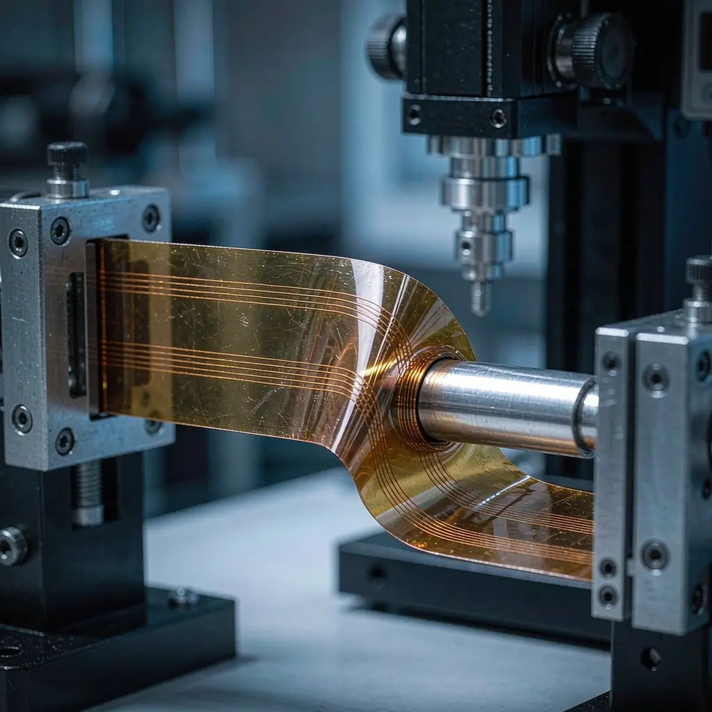
R = 3 mm Dynamic Bend | 200,000+ Cycles | 90Ω ±10% Impedance Verified
- 25 µm PI + 0.5 oz RA Copper
- Full-Surface EMI Shielding > 60 dB
- 2-Layer FPC, 90Ω Differential
Request a Quick Quote
ISO 9001:2015
Certified Quality Control
IPC-6013
Class 3 Flex Standard
2-Layer FPC
25 µm PI + RA Copper
RoHS & CE
Fully Compliant
R = 3 mm Bend
200,000+ Cycles Verified
Flexible PCB Types by Layer Count & Shielding

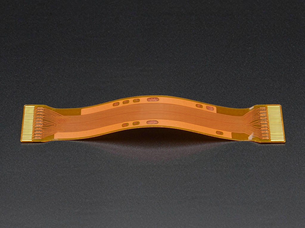
Single-Sided FPC
The simplest flex construction: one copper layer on a 25 µm polyimide film, sealed with coverlay and finished with gold fingers. It replaces discrete wires and ribbon cable in tight, low-cost interconnects.
- Lowest-cost route into flexible circuitry, fast to prototype
- One copper layer keeps the strip thin enough to fold inside a hinge gap
- Used for antenna feeds, button and camera links, sensor tails
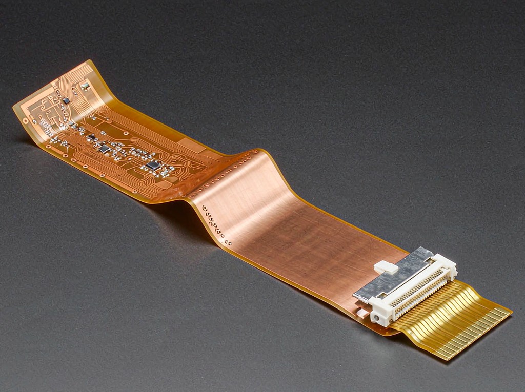
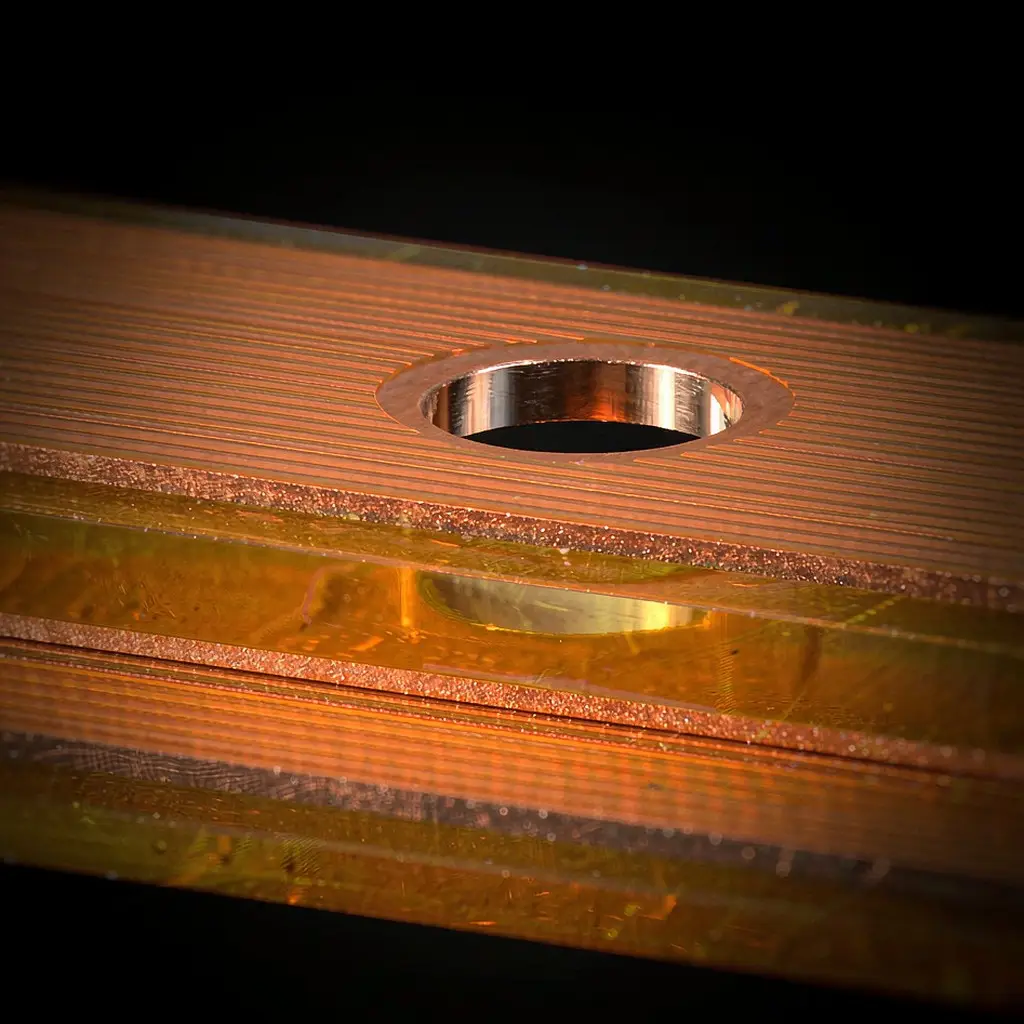
Double-Sided FPC
Two copper layers – one on each face of the PI film – joined by plated through-holes. Routing capacity doubles without adding thickness, which is what a foldable display bus needs for 90Ω differential pairs.
- Twice the routing density at the same finished thickness
- PTH and via structures hold impedance through the layer transition
- The workhorse build for foldable hinge and camera flex
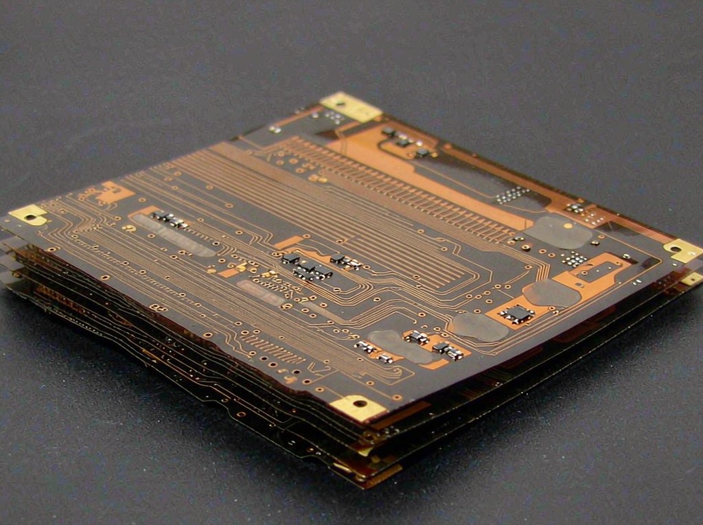
Multi-Layer FPC
Four or more laminated flex layers with blind and buried vias handle dense, impedance-controlled routing inside a single bendable assembly, including ground layers between the signal layers.
- Ground-signal-ground layers isolate high-speed buses inside the flex
- Blind and buried vias keep the outer faces free for component pads
- Used for multi-camera modules, wearables and medical probes
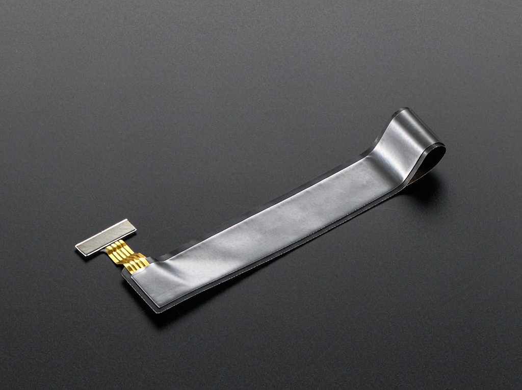
EMI-Shielded FPC
A silver-loaded shielding film is laminated over the coverlay and grounded to the flex ground plane, so the strip stops radiating and stops picking up noise without giving up its bendability.
- Continuous coverage across the whole strip, not just the trace area
- Grounded tab ties the shield to the flex ground plane
- Used in foldable handsets, camera modules and 5G antenna feeds
Rigid PCB vs Rigid-Flex PCB vs Flexible PCB (FPC)
FULL COMPARISON GUIDE (2026 FLEX ARCHITECTURE & SELECTION)
| KEY PARAMETERS | Rigid PCB Standard Board | Rigid-Flex PCB Hybrid Integration | RECOMMENDED Flexible PCB (FPC) Pure PI Film Circuit |
|---|---|---|---|
Base Material Substrate Composition | FR-4 / High-Tg FR-4 | Integrated FR-4 + Polyimide | Polyimide (PI) + RA Copper |
Flexibility & Motion Mechanical Behavior | Non-bendable(Rigid 2D Structure) | Bend-to-install(Rigid zones limit flexing) | 200,000+ Dynamic Bends(R = 3 mm hinge radius) |
Interconnect Method Board-to-Board Connections | Connectors, Headers & Wire Harnesses | ZIF Connectors or Direct Tail Soldering | No Harness, Direct Bonding |
Shock & Vibration Harsh Environment | Moderate Risk(Solder joint fatigue) | High Flexibility(Absorbs kinetic shock) | MAXIMUM Fatigue LifeNo solder joint inside the bend |
Cost Structure Bare Board vs. Total System | Bare Board: LowestHigh manual cable assembly | Bare Board: High(Hybrid lamination + stiffeners) | Bare Board: ModerateLowest Total Interconnect Cost(No harness, fewer joints) |
Primary Applications Best Use Cases | Consumer Electronics, Power Supplies, Motherboards | Wearable Modules, Camera Stacks, Medical Probes | Foldable Displays, Hinge FPC, Camera & Antenna Tails |
| Source: IPC-6013 / IPC-2223 flex design standards and 2026 foldable hinge reliability dataDESIGN & SELECTION MATRIX | |||
What is a Flexible PCB (FPC)?
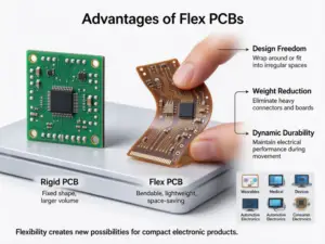
A flexible PCB is a circuit built on a thin polyimide film instead of a rigid laminate, so the whole board - traces, coverlay and stiffeners - can bend, fold or wrap around a hinge without a connector in between.
- Polyimide Substrate: 25 µm PI film carries the copper and survives hundreds of thousands of folds without cracking or delaminating.
- Rolled Annealed Copper: 0.5 oz RA copper has grains aligned in the plane of the film, so it resists fatigue under repeated dynamic bending.
- Coverlay & Shield: 25 µm PI coverlay seals the traces, and a shielding film grounds external noise on foldable designs.
Key Advantages
- Dynamic Bend Endurance: RA copper plus a thin PI build survives 200,000+ hinge cycles at R = 3 mm without a trace fracture.
- Space & Weight: A 0.1 – 0.2 mm strip replaces a wire harness and its connectors inside a hinge or camera stack.
- Controlled Impedance: 90Ω ±10% differential pairs hold their target right through the bend zone once the stackup is fixed.
- EMI Immunity: Full-surface shielding film holds attenuation above 60 dB from 100 MHz to 6 GHz.
Why Choose Flexible PCBs
Our engineering team pairs 25 µm PI, RA copper and full-surface shielding, so foldable hinge designs reach volume beyond 200,000 bend cycles.
- 200,000+ Bend Cycles
R = 3 mm dynamic bend verified without trace fracture or impedance drift
- 90Ω ±10% Impedance
Differential pairs held in spec through the flex zone and the stiffener transition
- > 60 dB Shielding
Full-surface EMI film blocks intra-device interference up to 6 GHz
- 0.15 mm PI Stiffeners
Stiffeners sit under SMT zones only, keeping the bend zone component-free
Core Advantages
Bend Zone Discipline: Traces run perpendicular to the bend line, with no vias or pads inside the bend and coverlay openings shifted off the centreline.
Ductile Conductor Choice: RA copper on an adhesiveless PI laminate gives fatigue life that ED copper cannot reach at R = 3 mm.
Shielding Without Stiffening: A thin silver-loaded film grounds the flex without adding a rigid layer, so attenuation rises and bendability stays.
Impedance Held Through Bending: TDR data from every lot confirms 90Ω ±10% before and after 200,000 bend cycles.
Proven Case Study
What is flexible PCB design?

Target Application
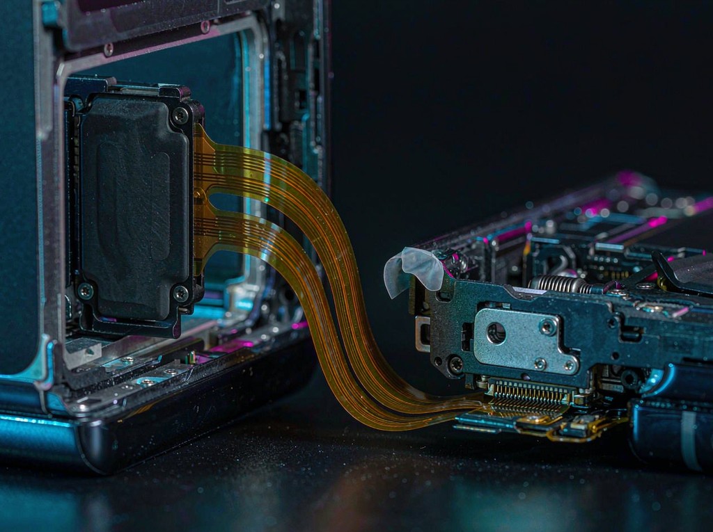
Foldable Smartphone Display Hinge FPC (2-Layer)
Technical Challenge
A display bus had to cross a 3 mm hinge radius more than 200,000 times while holding 90Ω ±10% differential impedance, with no room for a connector in the hinge gap and strict EMI limits inside the handset.
Structure
2-layer FPC on 25 µm PI, 0.5 oz RA copper, PI coverlay and a full-surface EMI shielding film.
Slpcba Manufacturing Solution
- ✓ Material Selection: 25 µm adhesiveless polyimide laminate with 0.5 oz rolled annealed copper, chosen for a grain structure aligned to the bend axis.
- ✓ Flex Zone Optimization: Traces routed perpendicular to the bend line, no vias or pads in the bend zone, and coverlay openings shifted off the centreline.
- ✓ Stiffener Design: 0.15 mm PI stiffeners behind the connector and SMT lands, so solder joints never see hinge strain.
- ✓ DFM Review: Pre-production DFM covering bend radius, copper grain direction, 90Ω stackup targets and stiffener placement.
Verified Results
- ✔ 220,000 Bend Cycles: Passed 220,000 dynamic bends at R = 3 mm with no line fracture and under 5% impedance shift.
- ✔ EMI Shielding: Shielding effectiveness above 60 dB at 1 GHz, measured across the 100 MHz to 6 GHz sweep.
- ✔ 90Ω ±10% Held: TDR verified before and after bending, with impedance coupons on every panel.

Why Choose Slpcba
Built for Foldable Hinge Life and 90Ω Signal Fidelity
200,000+ Bend Cycles
RA copper and a 25 µm PI build survive repeated R = 3 mm folding without micro-cracking.
90Ω ±10% Impedance
Differential pairs held in spec through the flex zone, verified by TDR on every lot.
> 60 dB EMI Shield
Full-surface shielding film grounds external noise from 100 MHz to 6 GHz.
100% Bend & AOI Testing
AOI, E-test, microsection and dynamic bend sampling before every shipment.
Ready to Build Your Flexible PCB?
Upload your Gerber and flex stackup today for a free DFM review and a detailed FPC quote within 24 hours.
Request a Quick Quote
Upload your Gerber files — DFM review & quote within 24 hours.
Engineering Capability
Technical Specifications & DFM Capabilities
| Parameter | Metric Value | Imperial Value | Feature Highlights |
|---|---|---|---|
| Layer Count | 2 Layers | 2 L FPC | Foldable Hinge Stackup |
| Min. Base Film | 0.025 mm | 0.001" | 25 µm Polyimide Film |
| Min. Trace / Space | 0.075 mm | 0.003" | Fine-Line Flex Patterning |
| Smallest Drill | 0.100 / 0.075 mm | 0.004" / 0.003" | Mechanical & Laser Via |
| Max Aspect Ratio | 5 : 1 | 5 : 1 | Plated Flex Through-Holes |
| Copper Weight | 0.5 oz (17 µm) | 0.5 oz | Rolled Annealed Copper |
| Flex Zone Stiffener | 0.15 mm PI | Custom Stiffeners | Strain-Free SMT Zones |
Premium Substrates & Surface Finishes
- Base Material: 25 µm adhesiveless polyimide laminate with 0.5 oz rolled annealed (RA) copper
- Coverlay & Shield: 25 µm PI coverlay plus a silver-loaded EMI shielding film, grounded to the flex plane
- Surface Finishes: ENIG, ENEPIG, Immersion Silver, OSP, Selective Hard Gold
Surface Treatment Options
✔ ENIG (Electroless Nickel Immersion Gold)
✔ ENEPIG (Electroless Nickel Electroless Palladium Immersion Gold)
✔ Immersion Silver
✔ Immersion White Tin
✔ OSP (Shikoku F2)
✔ OSP (Entek)
✔ Electrolytic Soft Gold
✔ Electrolytic Hard Gold
✔ Selective Hard Gold
✔ Bondable Gold (Wire Bonding)
✔ Gold Finger (30 µin Hard Gold)
FPC Fabrication Tolerances
| Parameter | Metric Value | Imperial Value |
|---|---|---|
| Min Base Film Thickness | 0.025 mm | 0.001″ |
| Min Trace / Space | 0.075 mm | 0.003″ |
| Min Coverlay Opening | 0.20 mm | 0.008″ |
| Dynamic Bend Radius | 3 mm | R = 3 mm |
| Verified Bend Cycles | 200,000 | 220,000 Achieved |
| Max FPC Thickness | 0.20 mm | 0.008″ |
| Layer Count | 1 – 6 L FPC | Multi-Layer Capable |
| Min Coverlay Thickness | 0.025 mm | 0.001″ |
| Stiffener Thickness | 0.15 mm | PI / FR4 / Steel |
| Impedance Coupons | 6 per panel | 100 % tested |
| Material Type | Example / Subtype | Function |
|---|---|---|
| Conductors & Shielding | Rolled Annealed (RA) Copper | 0.5 oz RA foil with grains aligned to the bend axis. This is the copper that survives 200,000 dynamic bends without micro-cracking. |
| Silver-Loaded Shielding Film | Laminated over the coverlay and grounded to the flex plane, holding attenuation above 60 dB from 100 MHz to 6 GHz. | |
| Coverlay & Stiffeners | PI Coverlay | 25 µm polyimide coverlay with a matching adhesive, sealing the traces while keeping the strip thin enough to fold. |
| PSA Bonding Layer | Pressure-sensitive adhesive for attaching stiffeners and mounting the FPC, used outside electrically active zones. | |
| PI Stiffener | 0.15 mm polyimide stiffener behind connectors and SMT lands, adding local rigidity without killing bendability. | |
| Stainless Steel Stiffener | For ZIF contacts that need extra wear resistance, bonded through the same PSA process. | |
| Conductive Adhesive | Bonds the shielding film and grounding tabs to the flex ground plane with low, stable contact resistance. | |
| Gold Finger / ZIF Bonding | Gold-finger and hot-bar land designs for direct bonding to the display or main board without a connector. | |
| Dielectric Families | Polyimide (PI) 25 µm | Tg above 250 °C, dimensionally stable and ductile. The default substrate for dynamic flex and foldable hinge FPCs. |
| Adhesiveless PI Laminate | Polyimide cast directly onto the copper foil. No adhesive interface means better flex life and lower Z-axis expansion. | |
| High-Tg Epoxy Stiffener | Rigid stiffener material for SMT zones that need FR-4 mechanical behaviour inside a flex assembly. | |
| Halogen-Free PI | RoHS and halogen-free polyimide for consumer brands with restricted-substance requirements. |
FAQ
Frequently Asked Questions About Flexible PCBs
A flexible PCB is built on a thin polyimide film instead of a rigid FR-4 laminate, so the circuit itself can bend, fold or wrap around a hinge. A rigid board needs a connector and a cable to reach a second board; an FPC reaches it in one continuous piece.
Rolled annealed copper is rolled, so its grains lie along the bend axis and it resists fatigue under repeated flexing. Electro-deposited copper grows vertically, which suits fine lines on rigid boards but cracks earlier under dynamic bending.
Stackup first: A 25 µm PI base with 0.5 oz RA copper and a 25 µm coverlay keeps the neutral axis centred through the bend.
Layout second: Traces run perpendicular to the bend line, with no vias, pads or coverlay openings inside the bend zone.
Verified third: Every design is sampled on a servo bending rig at R = 3 mm, and impedance is re-measured after the run.
A silver-loaded film is laminated over the coverlay and grounded to the flex plane, so it grounds external noise and stops the internal traces from radiating, holding attenuation above 60 dB without stiffening the strip.
PI, FR4 or stainless stiffeners add local rigidity behind connectors, ZIF sockets and SMT lands, so solder joints never see hinge strain while the rest of the strip stays fully bendable.
We build 3 mil (0.075 mm) line and space and 0.075 mm laser vias in volume on 25 µm PI. Finer geometries are available as a development capability, not as a standard production specification.
Bend-line violations dominate: vias or pads inside the bend, traces running parallel to the bend line, ED copper on a dynamic zone, or a bend radius below ten times the flex thickness.
Please send Gerber data, the flex stackup with coverlay and stiffener definitions, bend radius and bend direction, impedance targets, surface finish and quantity.
Yes. Each lot can ship with dynamic bend data at R = 3 mm, TDR impedance profiles, microsection images and AOI results.
Our factories hold ISO 9001, ISO 14001, UL and RoHS certification, and flex boards are built to IPC-6013 Class 3 with IPC-2223 design rules.
FPC thickness follows the layer count and the stiffener scheme:
1 – 2 layer FPC: typically 0.10 – 0.15 mm (0.004 – 0.006″);
4 – 6 layer FPC range from 0.20 – 0.40 mm (0.008 – 0.016″), commonly 0.20 mm (0.008″).
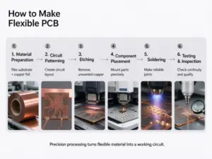
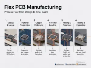
Polyimide cores are etched and laminated with coverlay, stiffeners are bonded, then the panel runs through lamination, plating, surface finish, outline routing and 100% electrical test before dynamic bend sampling.
Common builds include single-sided and double-sided FPC, 4 – 6 layer multi-layer flex, EMI-shielded FPC, semi-flex and rigid-flex, plus ZIF and hot-bar bonding tails.
Keep the bend zone free of vias, pads and coverlay openings, run traces perpendicular to the bend line, hold the bend radius above10 – 12 x the flex thickness for dynamic flex, and use hatched copper planes instead of solid planes in the bend zone.