High-Precision Rigid PCB Manufacturing & Quick-Turn Assembly
1 – 40 Layers | 3/3 mil Lines | ±2 mil | 99%+ Yield
- 1 – 40 Layer FR-4 / Rogers Stackup
- 3/3 mil Lines, ±2 mil Registration
- 24-Hour Prototype, 99%+ Volume Yield
Request a Quick Quote
ISO 9001:2015
Certified Quality Control
IATF 16949
Automotive QMS
IPC Class 2 & 3
Fabrication Standard
RoHS & CE
Fully Compliant
100% E-Test
TDR Impedance Verified
Rigid PCB Types by Layer Count & Construction

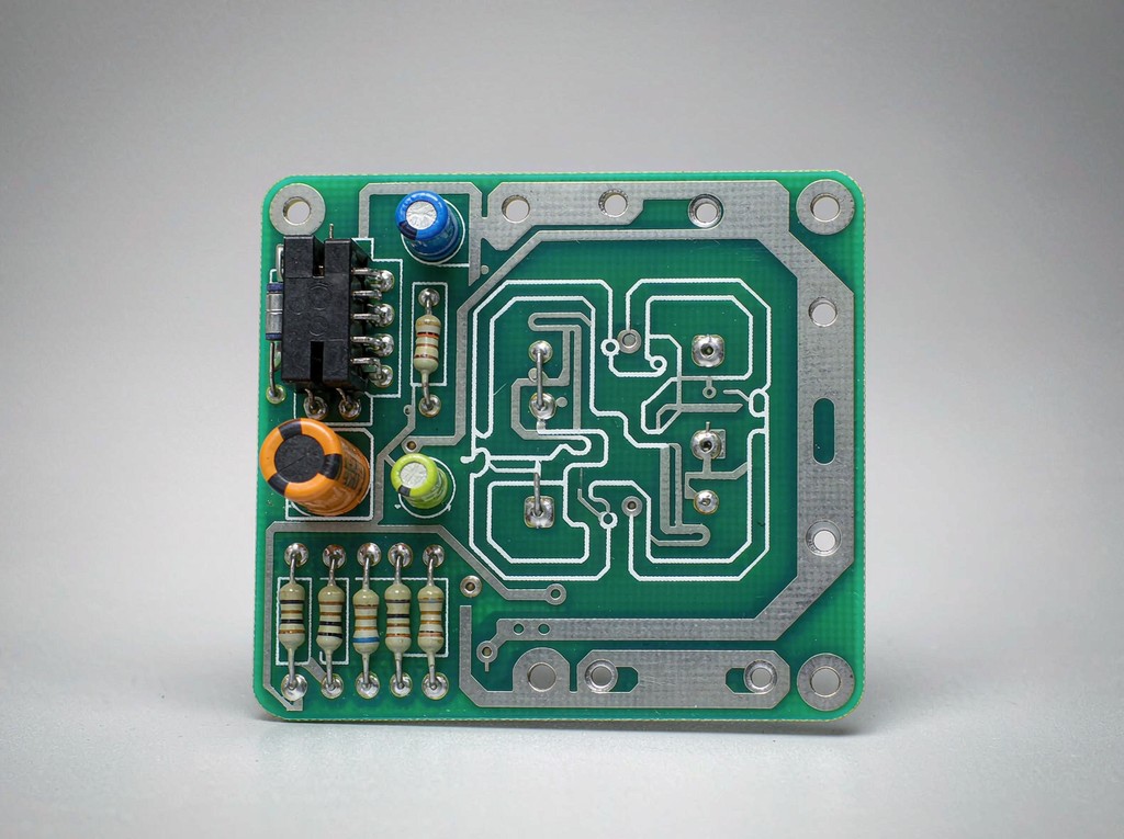
Single-Sided Rigid PCB
One copper layer on an FR-4 core, imaged and etched on a single face. It is the cheapest rigid construction to tool and the fastest to turn around, which still makes it the default for simple control, power and display boards.
- Lowest unit cost and the shortest lead time of any rigid build
- A single routing face keeps the board thin and panel yield high
- Used for power supplies, LED drivers, relays and simple control boards
Double-Sided Rigid PCB
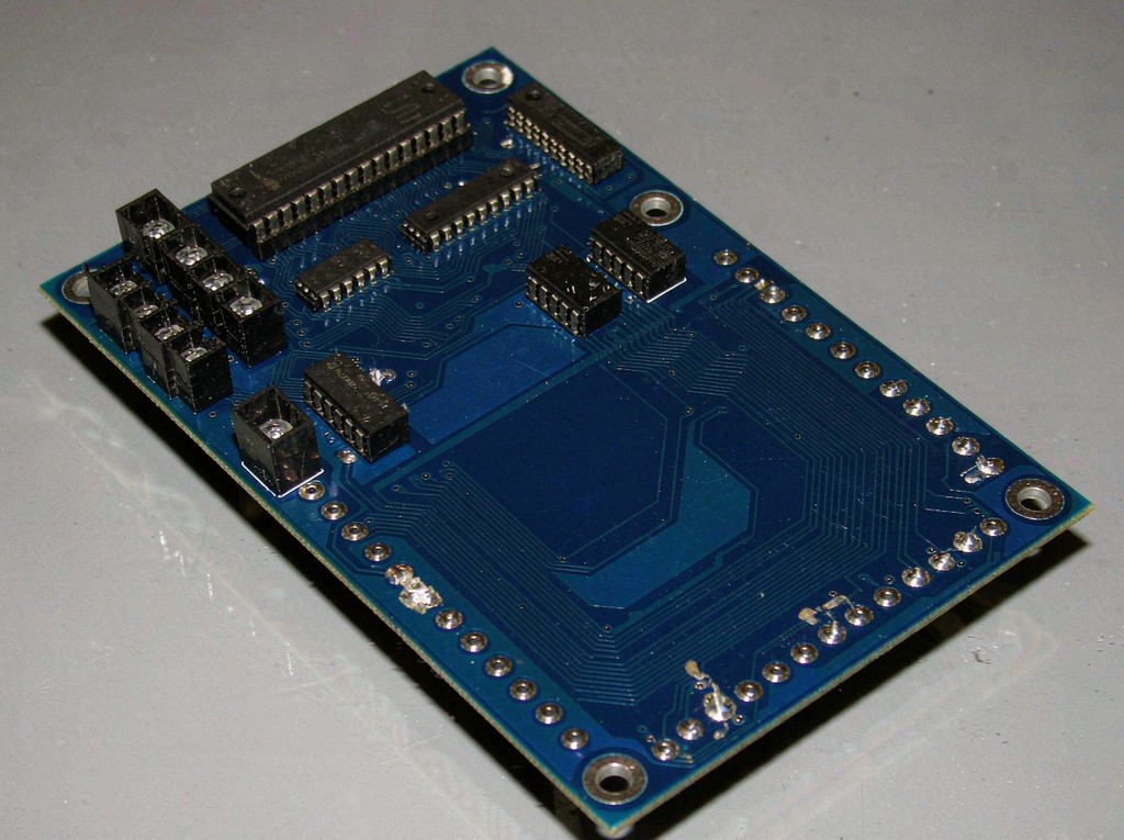
Two copper layers joined by plated through-holes, so traces can cross and route on both faces. It doubles the routing capacity of a single-sided board without extra lamination cycles, and still prototypes in 24 hours.
- Twice the routing area for a modest cost increase
- PTH barrels carry current and signals between the two faces
- The workhorse for industrial control, automotive body and IoT boards
Multi-Layer Rigid PCB
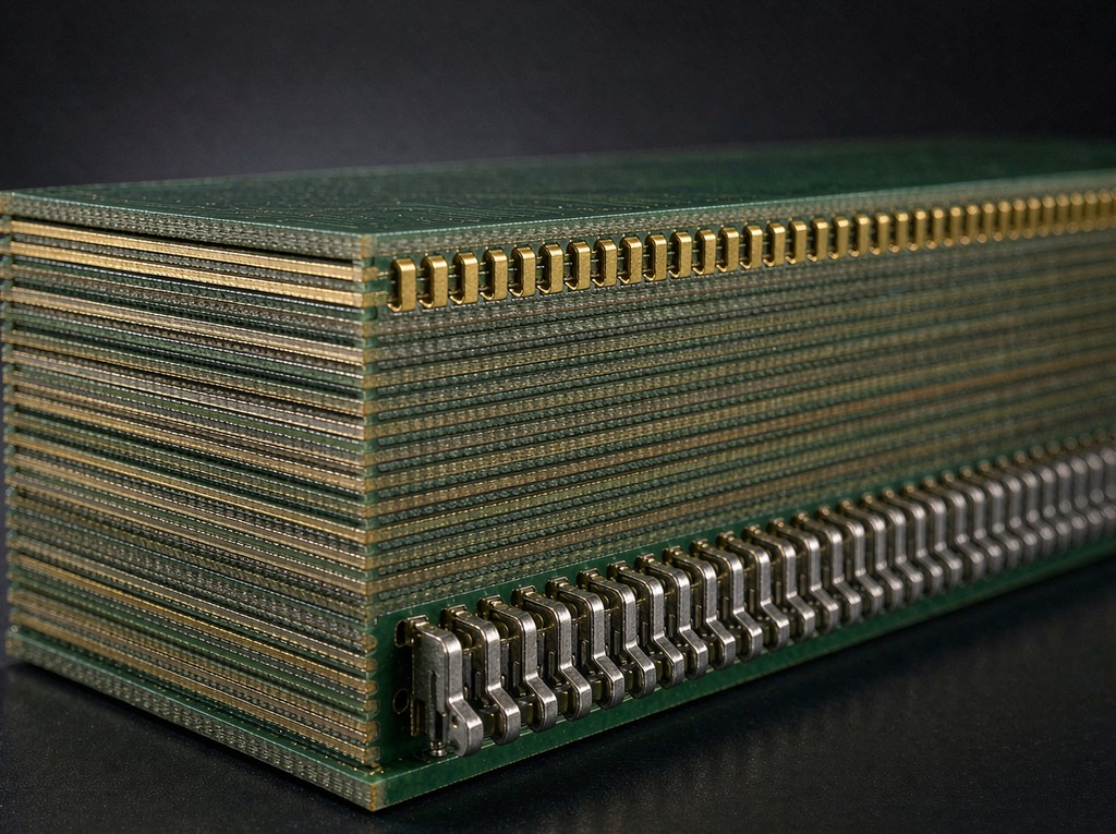
Four to forty copper layers laminated with prepreg, separated by dedicated ground and power planes. Blind and buried vias free up surface area, and controlled-impedance stackups hold signal integrity on high-speed buses.
- Dedicated ground planes cut EMI and hold controlled impedance
- Blind and buried vias keep the outer layers free for fine-pitch parts
- Used for backplanes, servers, telecom, medical and EV controllers
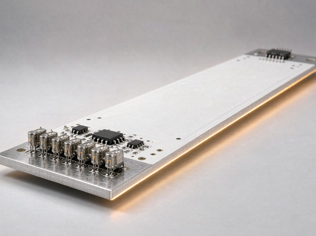
Metal-Core Rigid PCB
A single or double-sided circuit bonded to an aluminium or copper core through a thermally conductive dielectric. Heat leaves the LED or power device straight into the metal, so junction temperatures drop where FR-4 would discolour.
- Thermal resistance down to 1.0 °C/W through the dielectric
- Aluminium core for LED lighting, copper core for high-power modules
- Used in LED arrays, motor drivers, power conversion and EV chargers
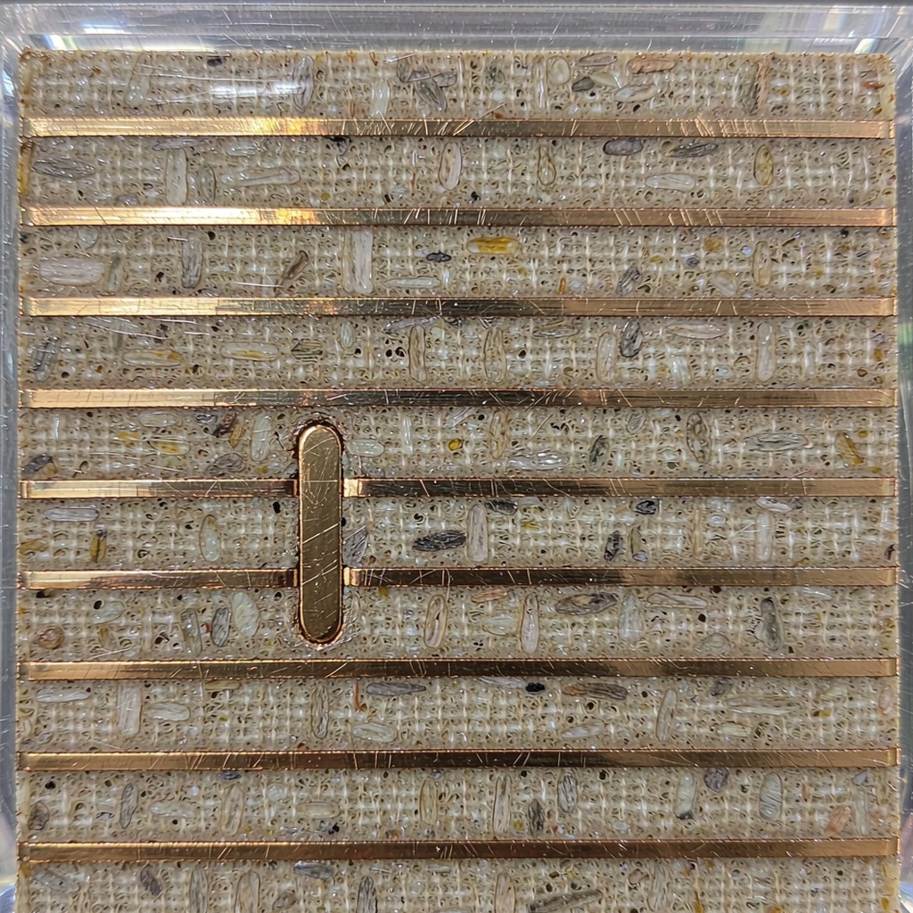
Standard Rigid PCB vs High-Layer Rigid PCB vs Rigid PCB + Assembly
FULL COMPARISON GUIDE (2026 LAYER COUNT & TURNKEY SELECTION)
| KEY PARAMETERS | Standard Rigid PCB 2 – 8 Layers | High-Layer Rigid PCB 12 – 40 Layers | RECOMMENDED Rigid PCB + Assembly Board + SMT, One Supplier |
|---|---|---|---|
Base Material Substrate Composition | FR-4 / High-Tg FR-4 | High-Tg FR-4 + Rogers Hybrid | FR-4 / Metal Core + BOM Kitting |
Stackup Depth Layer Count & Planes | 2 – 8 Layers(2 – 4 lamination cycles) | 12 – 40 Layers(6 – 20 lamination cycles) | Any Layer Count(fabricated and assembled) |
Interconnect Method Board-to-Board Connections | Connectors, Headers & Wire Harnesses | Press-Fit & Backplane Connectors | Direct SMT + THT, No Hand-Off |
Shock & Vibration Harsh Environment | Moderate Risk(Solder joint fatigue) | Higher Mass(Needs mechanical support) | MITIGATEDUnderfill + Conformal Coating |
Cost Structure Bare Board vs. Total System | Bare Board: LowestHigh volume unit cost | Bare Board: Higher(more laminations, lower yield) | Lowest Total Program CostOne BOM, one freight, one QA gate(Fewer suppliers, fewer escapes) |
Primary Applications Best Use Cases | Consumer, Power Supplies, LED Drivers | Backplanes, Servers, EV Controllers, Medical | Automotive ECUs, Industrial Box Builds, Turnkey Programs |
| Source: IPC-6012 / IPC-2221 rigid board standards and 2026 volume yield data from Slpcba production linesDESIGN & SELECTION MATRIX | |||
What is a Rigid PCB?
A rigid PCB is a circuit built on a stiff FR-4 or composite laminate. The base never bends, so heavy components, press-fit connectors and dense multi-layer stackups stay mechanically stable through assembly, reflow and years of service.
- FR-4 Substrate: Woven glass cloth in epoxy resin gives the board its stiffness, its UL 94 V-0 flame rating and its dimensional stability through reflow.
- Copper & Plating: 1 – 4 oz copper carries the current, and plated through-holes or vias connect the layers through a reliable, solderable barrel.
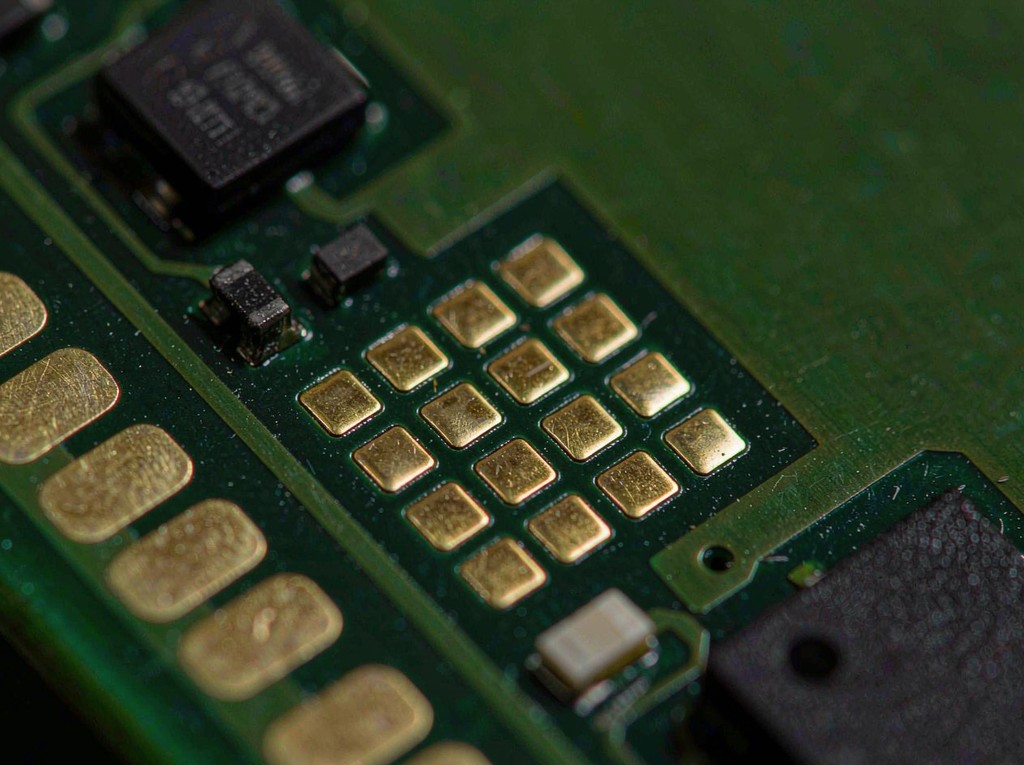
- Mask, Legend & Finish: Solder mask, silkscreen legend and an ENIG or HASL finish protect the copper and keep every pad solderable after storage.
Key Advantages
- Mechanical Stability: A non-bending base holds heavy transformers, press-fit connectors and large BGAs in place without stiffeners or carriers.
- Cost & Scalability: Standard FR-4 panels and mature processes make rigid boards the cheapest route from prototype to high-volume production.
- Layer & Routing Freedom: Up to 40 layers with dedicated ground and power planes allow fine-line routing, controlled impedance and effective shielding.
- Thermal Endurance: High-Tg laminates and metal-core options stay stable above 130 °C and survive lead-free reflow at 260 °C.
Why Choose Rigid PCBs
Our engineering team pairs 1 – 40 layer fabrication with 3/3 mil fine lines and ±2 mil registration, so rigid boards reach volume above a 99% yield.
- 1 – 40 Layers
Single-sided prototypes through 40-layer backplanes on one fabrication line
- 3/3 mil Fine Lines
LDI imaging and advanced etching hold 75 µm line and space in volume
- ±2 mil Registration
CCD target punching and X-ray checks keep layer-to-layer alignment tight
- 99%+ Volume Yield
SPC-monitored etching, AOI and 100% E-test on every panel
Core Advantages
Layer Count Without Compromise: One shop covers 1 to 40 layers, so the stackup you qualify in prototype is the stackup you scale in volume.
Fine-Line Precision at Volume: 3/3 mil lines with ±2 mil registration let a 0.4 mm pitch BGA escape on a standard rigid build.
Certified Quality System: ISO 9001 and IATF 16949 processes with AOI, X-ray, TDR and microsection on every lot.
Turnkey Fabrication + Assembly: Bare board, component sourcing and SMT/THT assembly under one roof shorten the program schedule.
Proven Case Study
What is rigid PCB manufacturing?

Target Application
12-Layer Automotive ADAS Radar Control Board
Technical Challenge
A 12-layer board had to carry 0.4 mm pitch radar SoCs and 2 oz power planes on one stackup, hold ±2 mil layer registration, pass AEC-Q100 grade 2 thermal cycling, and still yield above 99% in volume.
Structure
12-layer rigid FR-4 (Tg 170 °C), 1 oz inner / 2 oz outer copper, ENIG finish.
Slpcba Manufacturing Solution
- ✓ Material Selection: High-Tg 170 °C FR-4 cores with 1080 / 2116 prepreg, chosen so a 12-layer stackup holds thickness and registration through six lamination cycles.
- ✓ Stackup & Impedance: Dedicated ground planes with 50 Ω single-ended and 100 Ω differential targets, simulated before release and verified by TDR coupons on every panel.
- ✓ Surface Finish & Thermal: ENIG for the 0.4 mm pitch BGA lands, with 2 oz copper on the power layers to spread heat away from the radar SoC.
- ✓ DFM Review: Pre-production DFM covering annular ring, aspect ratio, solder-mask dam width and panel utilisation before the first lot.
Verified Results
- ✔ 99.4% Volume Yield: Five production lots held above 99% first-pass yield, with AOI and 100% E-test on every panel.
- ✔ ±1.6 mil Registration: Layer-to-layer alignment measured at ±1.6 mil, inside the ±2 mil target across all 12 layers.
- ✔ Thermal Cycling Passed: 1,000 cycles from -40 to +125 °C with no barrel crack, meeting AEC-Q100 grade 2.
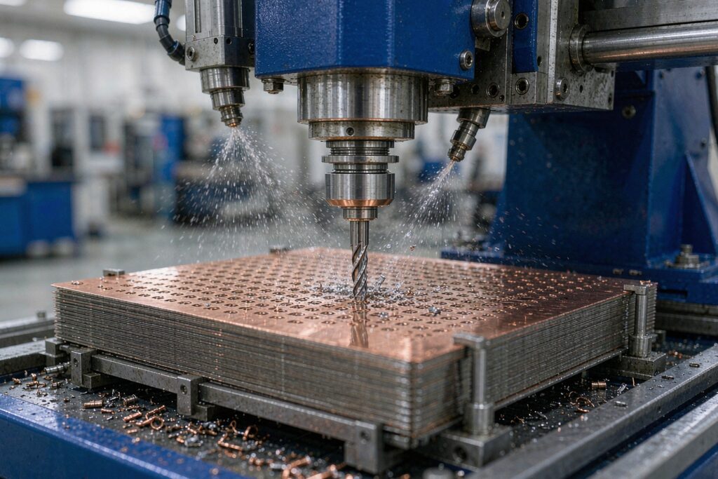
Why Choose Slpcba
Built for Layer Count, Fine Lines and Repeatable Volume Yield
1 – 40 Layers
One line covers single-sided prototypes through 40-layer backplanes, so the stackup you qualify is the stackup you scale.
3/3 mil Fine Lines
LDI exposure with advanced etching holds 75 µm line and space in volume, not only in the lab.
±2 mil Alignment
CCD target punching and X-ray registration checks keep every layer inside tolerance.
Full-Stage QC
AOI, X-ray, flying-probe E-test, TDR and microsection on every lot before shipment.
Ready to Start Your Rigid PCB Project?
Upload your Gerber files today for a free DFM review, a stackup proposal and a detailed quote within 24 hours.
Request a Quick Quote
Upload your Gerber files — DFM review & quote within 24 hours.
Engineering Capability
Technical Specifications & DFM Capabilities
| Parameter | Metric Value | Imperial Value | Feature Highlights |
|---|---|---|---|
| Layer Count | 1 – 40 Layers | 1 – 40 L | Rigid FR-4 & Hybrid Stackup |
| Min. Trace / Space | 0.075 mm (3 mil) | 0.003" | Fine-Line LDI Imaging |
| Layer-to-Layer Alignment | ±0.050 mm | ±2 mil | CCD Punch & X-Ray Verified |
| Smallest Drill (Mech / Laser) | 0.15 mm / 0.075 mm | 0.006" / 0.003" | Microvia & Blind / Buried |
| Max Aspect Ratio | 20 : 1 | 20 : 1 | Reliable Plated Through Holes |
| Finished Copper Weight | Up to 4 oz (140 µm) | Up to 4 oz | Heavy Copper Power Planes |
| Board Thickness | 0.4 – 3.2 mm | ±10% | Rigid Panel, No Warpage |
Premium Substrates & Surface Finishes
- Base Material: High-Tg FR-4 (Tg 150 – 180 °C), Rogers RO4350B / RO4003C and Taconic TLY for RF sections
- Copper & Build: 1 – 4 oz ED copper, 1080 / 2116 / 7628 prepreg, blind and buried vias on 12+ layer builds
- Surface Finishes: ENIG, Lead-Free HASL, Immersion Silver, OSP, Hard Gold
Surface Treatment Options
✔ ENIG (Electroless Nickel Immersion Gold)
✔ ENEPIG (Electroless Nickel Electroless Palladium Immersion Gold)
✔ Lead-Free HASL
✔ Immersion Silver
✔ Immersion White Tin
✔ OSP (Shikoku F2)
✔ OSP (Entek)
✔ Electrolytic Soft Gold
✔ Electrolytic Hard Gold
✔ Selective Hard Gold
✔ Gold Finger (30 µin Hard Gold)
Rigid PCB Fabrication Tolerances
| Parameter | Metric Value | Imperial Value |
|---|---|---|
| Min. Trace / Space | 0.075 mm | 3 mil |
| Layer-to-Layer Alignment | ±0.050 mm | ±2 mil |
| Min. Mechanical Drill | 0.15 mm | 0.006″ |
| Min. Laser Drill | 0.075 mm | 0.003″ |
| Max Board Thickness | 3.2 mm | 0.126″ |
| Min. Board Thickness | 0.4 mm | 0.016″ |
| Max Layer Count | 40 Layers | Rigid Multi-Layer |
| Impedance Tolerance | ±8 % | TDR Verified |
| Copper Weight | 1 – 4 oz | 35 – 140 µm |
| Max Panel Size | 520 × 620 mm | 20.5″ × 24.4″ |
| Material Type | Example / Subtype | Function |
|---|---|---|
| Conductors | ED Copper (1 – 4 oz) | Electro-deposited foil is the standard conductor on rigid boards. It holds fine lines well and is available up to 4 oz for power planes and heavy-current traces. |
| RA Copper (High Reliability) | Rolled annealed foil is used where thermal cycling is severe. Its grain structure resists cracking at plated through-holes in automotive and aerospace builds. | |
| Laminates & Prepreg | High-Tg FR-4 | Tg 150 – 180 °C cores keep the board dimensionally stable through lead-free reflow and repeated thermal cycling. |
| Rogers RO4350B | Low-loss laminate (Dk 3.48, Df 0.0037) for RF and antenna sections that standard FR-4 cannot hold. | |
| Taconic TLY | Ultra-low loss laminate for microwave and satellite hardware where insertion loss has to stay minimal. | |
| FR-1 / FR-2 Phenolic | Paper-based laminate for cost-sensitive consumer boards that see no thermal or mechanical stress. | |
| Aluminium Metal Core | Circuit bonded to an aluminium core through a thermally conductive dielectric, pulling heat out of LED and power devices. | |
| Bonding Prepreg (B-Stage) | 1080 / 2116 / 7628 glass styles that set dielectric thickness and resin flow during lamination, which is what holds ±2 mil registration on thick stackups. | |
| Surface Finishes & Mask | ENIG | Electroless nickel with an immersion gold top layer: flat, solderable and stable for fine-pitch BGA and long storage. |
| Lead-Free HASL | Hot-air levelled tin-silver-copper finish, the most economical option for through-hole and coarse-pitch SMT boards. | |
| Immersion Silver | Silver finish with excellent solderability for fine lines and press-fit connectors, and a flat pad profile. | |
| OSP | Organic solderability preservative: an invisible, flat coating for boards assembled inside a short window. |
FAQ
Frequently Asked Questions About Rigid PCBs
A rigid PCB is a circuit built on a stiff FR-4 or composite laminate that never bends. It carries components, connectors and multi-layer routing in one mechanically stable assembly, which is why it is the default for consumer electronics, power supplies, industrial control, automotive and telecom hardware.
Standard 2 – 6 layer prototypes ship in 24 hours, while volume orders run 2 to 7 business days depending on layer count, copper weight and special processes such as blind vias or impedance control.
2 layers: single or double-sided routing for simple control boards, LED drivers and power supplies, at the lowest unit cost.
4 – 8 layers: dedicated ground and power planes for impedance control and EMI, the sweet spot for industrial, IoT and automotive body electronics.
12 – 40 layers: backplanes, servers, radar and EV controllers where routing density, shielding and fine-pitch BGA escape all matter at once.
Choose Rogers when the board runs above roughly 1 GHz or in RF front-ends: FR-4 loses Dk stability and dissipates more energy at those frequencies, while RO4350B holds Dk 3.48 and Df 0.0037 across frequency and temperature.
ENIG or immersion silver for BGA pitch below 0.5 mm: both give a flat, planar pad that HASL cannot match, and ENIG also survives long storage without oxidising. Lead-free HASL stays the economical choice for coarse-pitch and through-hole work.
3/3 mil (75 µm) line and space with 0.15 mm mechanical drills and 0.075 mm laser vias in volume. Tighter geometry is available as a development capability, not as a standard production specification.
Laser direct imaging, CCD target punching and X-ray registration checks after lamination. Every lot is measured against the ±2 mil target before etching, which keeps annular rings and impedance inside tolerance.
Copper imbalance and asymmetric stackups are the main causes. We balance copper distribution per layer, use symmetric prepreg schedules, press at controlled ramp rates, then bake and measure flatness before routing.
Yes. Every lot can ship with TDR impedance profiles, microsection images, AOI and flying-probe results, plus thermal cycling data on request.
Yes. Bare board fabrication, component sourcing and SMT/THT assembly run under one roof, so a turnkey order arrives tested with one BOM, one freight and one quality gate.
Rigid board thickness follows the layer count and copper weight:
2 – 4 layer boards: typically 0.8 – 1.6 mm (0.031 – 0.063″);
12+ layer backplanes range from 2.0 – 3.2 mm (0.079 – 0.126″), commonly 1.6 mm (0.063″).
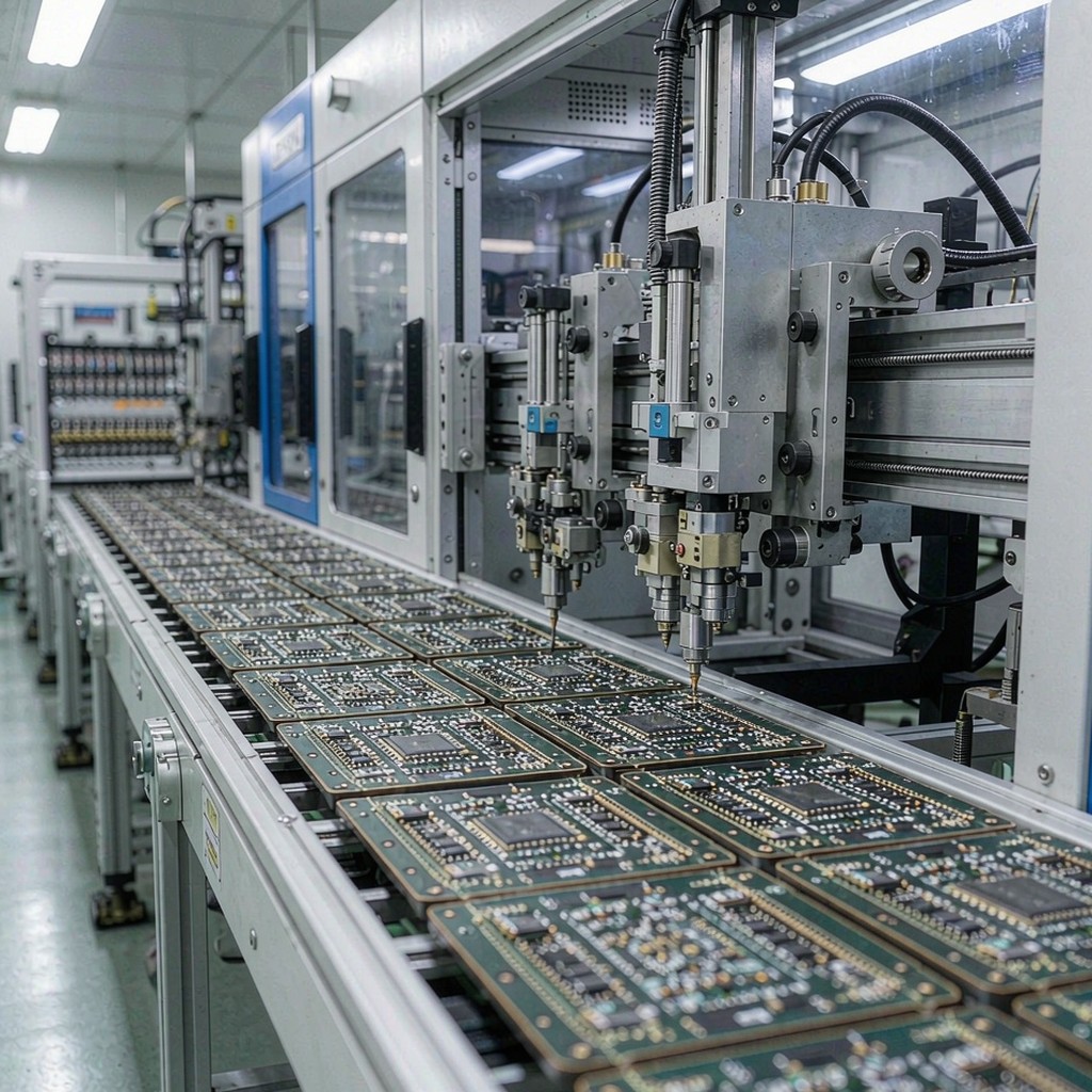
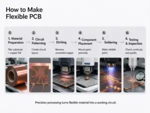
Inner layers are imaged, etched and AOI-checked, then laminated under heat and pressure, drilled, plated, imaged on the outer layers, solder-masked, surface finished, profiled and 100% electrically tested before packing.
ISO 9001, IATF 16949, UL and RoHS. Boards are built to IPC-6012 Class 2 or Class 3 depending on the application, with IPC-2221 design rules for stackup and clearance.
Keep annular rings at least0.05 mm on 0.15 mm drills, hold solder-mask dams above 0.1 mm, keep the aspect ratio at or below 20:1, and balance copper per layer so the panel stays flat through reflow.