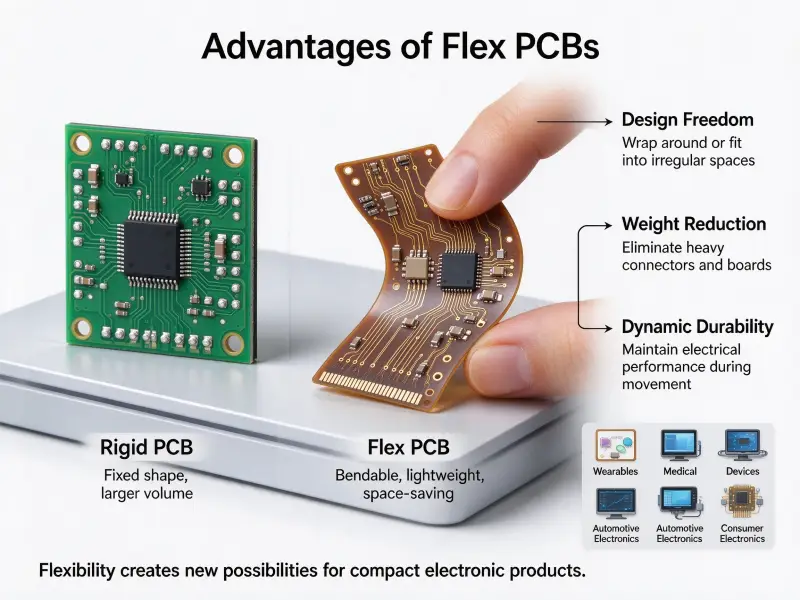
Rigid-flex boards turn up wherever a device must fold, twist, or survive vibration: instrument panels, medical handhelds, camera modules, automotive electronics, and wearable housings. The appeal is mechanical. One laminated board replaces the wire harness, the board-to-board connector, and the second PCB a rigid design would otherwise need. Buyers usually start by shortlisting a rigid-flex PCB manufacturer supplier that can run both halves of the process in one place, because the flex core and the rigid stack have to be engineered as one structure rather than joined afterward.
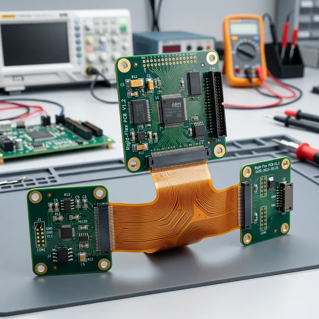
A rigid-flex PCB is made by building a flexible polyimide core separately—copper foil, drilled and plated vias, etched traces, and then a coverlay—and laminating that core between rigid FR-4 sections so the flex layers run continuously through the board while the rigid layers stop short of the bend zones. The board leaves lamination as one piece, with no connector, no crimp, and no flex cable soldered onto a rigid board.
What follows covers the process in order, then the design rules that decide whether the part survives its bend life.
What rigid-flex PCB manufacturing actually involves
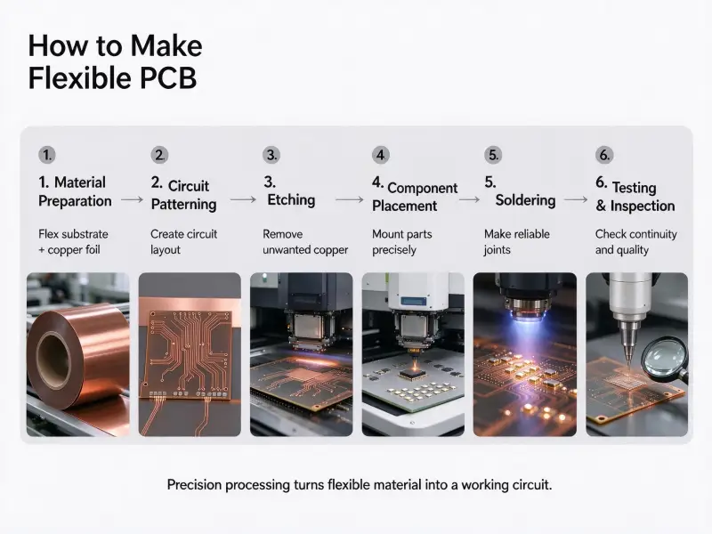
Rigid-flex manufacturing is a rigid PCB process and a flex circuit process running as two parallel halves that meet at lamination. Everything a rigid board goes through—imaging, etching, drilling, plating, solder mask, surface finish—happens here too. The flex half adds steps a rigid board never needs: a seed layer or adhesive, rolled copper foil, a polyimide coverlay instead of a solder mask, and mechanical blanking instead of panel routing.
That distinction drives lead time and price. A shop that ships the flex core to a subcontractor adds a transfer, an inspection, and a queue between two processes that must agree on drill registration. Panel utilization matters too, because framed flex sections must survive lamination unsupported, so boards nest with more air, and one off-register part scraps the panel.
Materials used in rigid flex PCB manufacturing
The flex section is a flexible dielectric film with copper on both faces; the rigid section is FR-4. Nothing else in the stackup is exotic, but the film choice sets the temperature rating, the bend life, and the cost.
| Material | Where it appears | What to watch |
| Polyimide (PI) film | Flex core dielectric | Standard flex material absorbs more moisture than other films, so it needs a bake-off before reflow. |
| Polyester (PET, PEN) | Sensor tails, LED strips | Cheap and easy to process, poor heat resistance, unsuitable for reflow-heavy products |
| PTFE film | High-frequency defense | Lowest dielectric constant and loss of the three, expensive and difficult to laminate |
| LCP film | 5G and mmWave modules | Low dielectric loss and low moisture uptake, less widely available |
| Adhesiveless PI | Flex core in most modern builds | No glue layer and better reliability, higher material cost, needs a plating seed |
| PI coverlay | Over the flex traces | Protects conductors and doubles as a solder mask where parts mount on flex |
| FR-4 core | Rigid sections | Carries components and connectors, no flex capability |
Published dielectric values differ enough to change a design. Polyimide runs a relative dielectric constant of roughly 3.4 to 3.5 with losses of 0.002 to 0.004 and takes 250 to 400 °C by grade, while polyester tops out near 150 to 180 °C (typical ranges for these film families, checked 10 October 2026).
The flex core build-up, step by step
The flex core is built as a small board on its own, through the same photolithography steps used on a rigid core, and it is blanked out of its frame before it ever meets the rigid stack. A fabricator may start from pre-laminated flex with foil already attached or from bare film.
- Adhesive or seed coat. An epoxy or acrylic adhesive goes on, or a thin copper seed layer is deposited by vacuum sputtering so plating has a key to grow on.
- Copper foil. Foil is laminated into the adhesive, which is the mainstream route, or chemically plated onto the seed layer. Adhesiveless processes bond rolled annealed foil with a tie coat.
- Drilling. Vias and pads are mechanically drilled, and multiple flex substrates can be drilled at once on reels. Pre-cut flex panels can be drilled between rigid blanks, though registration accuracy drops. Laser drilling is available for microvias at a premium, since each film is drilled separately.
- Through-hole plating. Copper is chemically plated as on a rigid core. Flex through-holes run 1 mil minimum to give the pad mechanical support, whereas a low-cost rigid board may run half that composite thickness.
- Etch-resist printing. A photosensitive resist is coated over the film, and the circuit pattern is exposed and developed.
- Etching and stripping. Exposed copper is etched away, then the resist is stripped off.
- Coverlay or covercoat. PI film is laminated over both faces and cut to shape, or a photo-imageable solder mask is printed onto the flex.
- Blanking. The circuit is cut from its frame. Volume production uses a hydraulic punch and die set, which carries real tooling costs but cuts many circuits at once. Prototypes use a blanking knife, a razor blade bent to the outline.
| Step | What goes wrong there? | Consequence |
| Seed coat and lamination | Poor adhesion, contamination | Voids under copper, delamination later |
| Drilling | Registration drift between blanks | Holes miss pads. |
| Plating | Under-thick barrel in the flex | Cracked pads after repeated bending |
| Etching | Trace undercut | Marginal copper at the bend |
| Blanking | Ragged cut edge, nicks | Stress risers where flex meets the bend |
Lamination: combining flex and rigid sections
The flex core is framed, positioned between rigid blanks, and pressed together with prepreg at heat and pressure so the two become one laminate. Each rigid panel is routed out where the flex is meant to be free, and flex sections are separated by rigid prepregs and cores or by PI bonding sheets carrying epoxy or acrylic adhesive.
The flex circuit needs a frame that keeps it flat through the press cycle, since unsupported flex elbows can distort in a later reflow oven. And adhesive layers expand in Z during reflow, so a flex core that shifts against the rigid stack can crack at the transition. That is why many designers now prefer FR-4 prepreg with thermosetting epoxy, which holds dimension better.
Embedded flex takes a different route. Flex circuit units are printed and embedded inside an internal rigid board, then built up through repeated lamination cycles, and flex and rigid circuits connect only through blind and buried vias. It cuts polyimide waste and lifts usable material area at the price of more fab complexity.

Rigid-flex PCB stackup design guidelines
Keep the flexible section as few layers as the electrical design allows, because every extra flex layer adds thickness, and thickness sets your minimum bend radius. The stackup also needs to stay reasonably symmetric around the neutral axis, or repeated thermal cycling will bow and twist the board.
| Build type | Typical arrangement | Fits |
| Two-layer flex with rigid sections | Two flex layers continuous through the board, rigid layers terminating at each end | Cable and harness replacement, moderate routing density |
| Multilayer flex | Four or more continuous flex layers | Dense routing inside the bend accepts a tighter radius. |
| HDI rigid-flex | Laser microvias, blind and buried vias, sequential lamination | Fine-pitch BGA fanout, compact modules |
| Embedded flex | Flex units buried inside a rigid core, joined by blind and buried vias | High layer count with small flex area |
Flex layers run through both zones without interruption, and the flex core is never FR-4. Rigid layers terminate at defined boundaries instead of drifting into the bend. Where high-speed lines cross the transition, account for the dielectric constant shift between polyimide and FR-4 when you calculate impedance.
Bend radius, copper, and transition zone rules
A bend radius of roughly six times the finished flex thickness handles a static bend, which is made once during assembly and then left in place. Repeated bending needs ten times that or more. These are commonly cited starting points, not a standard you can print on a drawing. Published guidance disagrees about dynamic applications, ranging from about 10:1 at one end to 100:1 and beyond at the other, so confirm the number your fabricator designs to before committing copper.
| Flex section construction | Static bend starting point | Dynamic bend starting point |
| Single-layer flex | 6× thickness | 12× thickness, more for high-cycle use |
| Two-layer flex | 10× thickness | 20× thickness |
| Multilayer flex | 12× thickness | 20× thickness or higher |
Radius is measured to the inside surface of the bend, where compression is highest, not to the centerline. Getting that wrong produces cracks that surface months later.
Copper choice decides how long a dynamic design lasts. Vendor-published elongation figures put rolled annealed copper at roughly 20 to 30 percent before fracture, against roughly 10 to 15 percent for electrodeposited foil (copper foil vendor ranges, checked 10 October 2026). Rolled grains elongate with the bend, while electrodeposited grains form a columnar structure that propagates cracks. Electrodeposited foil is still fine in rigid layers and static flex.
Inside the bend zone, the rules narrow fast. No components, no pads, no plated through-holes, since a rigid barrel in a dynamic bend cracks under repeated flexing. No solid copper pours, because a solid plane stiffens the flex; use a hatched ground pattern where you need a reference. No 90-degree corners, with traces running perpendicular to the bend axis in smooth curves. Stagger traces across layers rather than stacking one directly above the other.
The rigid-to-flex transition is the most mechanically stressed area on the board, and field failures cluster there. Taper the rigid section over 30 to 45 degrees rather than stepping down abruptly. Keep traces about 20 mil from the boundary edge and vias roughly 1 to 2 mm away in the rigid zone, more for dynamic flex. Round the transition with a fillet so stress spreads instead of concentrating, run the flex coverlay at least 30 mil onto the rigid section so it cannot peel back, and keep stiffeners clear of the bend tangent.
What drives rigid flex PCB cost?
Layer count drives rigid flex PCB cost more than anything else, and panel utilization plus yield decide the rest. Published industry guides put a rigid-flex board at roughly two to five times the price of an equivalent rigid board of the same outline area, with the spread widening on complex builds (public fabricator cost guides, checked 10 October 2026). Treat that as a directional range, not a quote.
| Cost driver | Why it moves the price |
| Total layer count | Each layer adds imaging, lamination, drilling, and inspection steps. |
| Flex layer count | Flex layers need polyimide, flex-specific processing, and separate registration control. |
| Material system | Adhesiveless and low-loss laminates cost more than adhesive-based FR-4 builds. |
| Copper foil and weight | RA copper and heavier copper raise material costs. |
| Panel utilization | Framed flex sections and routing air leave less usable area per panel. |
| Yield | Published estimates put complex rigid-flex yields around 70 to 85 percent, against 90 percent or better for standard rigid boards. |
| Tooling and volume | Blanking dies and test fixtures spread across the run, dominating a prototype and amortizing in production |
Cost per square inch is the wrong lens for a purchasing decision, because it ignores what the board replaces. A rigid-flex design that removes two connectors, one cable assembly, and the labor to install them is often the cheaper assembly overall, and it removes the connector pair that usually fails first. For a static bend or a low-cycle design, though, a rigid board with one connector is usually the right answer.
Inspection, testing, and standards compliance
Every rigid-flex board gets 100% electrical testing, and the purchase order should name the acceptance class before the job is priced. Standards language is where most disputes land, so put it in writing rather than in an email thread.
Design work falls under IPC-2223 for flex-specific rules and IPC-2221 for generic board design, with IPC-A-600 covering printed board acceptability. Qualification and performance for flex and rigid-flex construction sit in IPC-6013E, the current qualification and performance specification for flexible and rigid-flexible printed boards (IPC, verified 10 October 2026). It covers single-sided, double-sided, multilayer, and rigid-plus-flex constructions, and it defines three performance classes: Class 1 for general electronics, Class 2 for dedicated service products, and Class 3 for high-performance and harsh-environment equipment. Class 3 is not Class 2 with better luck. It tightens copper wicking limits, requires complete solder fillets, and adds inspection to the plan.
Inspection usually runs in this order:
- 100% electrical test for continuity and isolation on a fixture built for the panelization
- Impedance measurement by TDR where controlled impedance is specified
- Microsectioning on sampled lots to verify plating thickness and the rigid-to-flex interface
- Visual inspection under magnification for coverlay registration, cut edge quality, and exposed copper
- Bend testing on coupons for dynamic designs, run to the cycle count you specified
- Thermal stress testing, often to a stated number of reflow cycles, because polyimide absorbs moisture and a flex core is where a weak joint would show up
Questions to ask before you place a rigid-flex order
Send a complete package before you ask for a price, because most of the cost difference between two quotes for the same design is missing data. Worth raising in a flexible PCB supplier custom FPC capability review:
- Can you accept my stackup file, or do you need to propose one?
- Is this design rigid-flex, or would flex plus a connector be cheaper and more reliable?
- What bend ratio do you design to, static and dynamic, and how many bending cycles will you qualify for?
- Which copper foil do you use in the flex zone, RA or ED?
- Adhesiveless or adhesive-based flex core, and how does that change my lead time?
- Do you supply stiffeners, and can they be positioned in my transition zones?
- What is the coverlay material, and which performance class will the boards be inspected to?
- What do you need in the quote request: Gerbers, drill file, stackup, bend lines, and a drawing defining flex areas?
Mark bend lines and bend areas on a separate mechanical layer. State the bend radius and the expected cycle count, and define the flex area with a fabrication drawing that includes dimensional tolerances.
Frequently asked questions
Can a rigid-flex PCB be repaired after it fails?
Usually not, and that is the main practical argument for the technology. Small trace repairs on prototypes can sometimes be done with conductive epoxy or micro-soldering, but the repair sits in a mechanical stress zone and reduces reliability. In production, replacing the board is cheaper and safer.
How much longer does a rigid-flex lead time take than a rigid board?
Commonly one to three weeks longer than a comparable rigid order (published fabricator guidance, checked 10 October 2026), and more when the build needs sequential lamination, blind vias, or adhesiveless cores.
What is the minimum quantity for a rigid-flex build?
It depends on the tooling. A blanking die and a forming fixture have real costs, so prototypes run one piece at a time using a knife cut, while production runs justify the die.