Rigid-flex PCBs combine rigid and flexible substrates on one board, letting designers fold circuitry into tight three-dimensional enclosures without separate connectors or cables. Because the build is a partnership between design and factory capability, the first practical step is to learn what a rigid-flex PCB manufacturer supplier can hold in production before locking in a stack-up.
Rigid-flex PCB thickness is not a single fixed measurement. It is the sum of two independent regions: a rigid section, typically 0.4 to 2.4 mm, that carries components, and a flexible section, usually 0.05 to 0.3 mm, that bends to route signals in three dimensions. Total board thickness ranges from roughly 0.5 mm in thin builds to over 3.2 mm in high-layer-count designs, and the final number is set by layer count, copper weight, materials, stiffeners, and bend needs rather than by any universal standard.
The sections below break down the build by region, material, and design rule so you can specify a stack-up with confidence.

What Is a Rigid-Flex PCB and How Is Its Thickness Measured?
A rigid-flex PCB is a hybrid circuit that laminates flexible polyimide layers with rigid FR-4 sections so the board can both support components and bend. Its thickness is measured separately for the rigid and flexible regions because the two zones use different materials and serve different mechanical jobs, so one overall number hides what a designer actually needs.
Why Thickness Is Two Numbers, Not One
A conventional rigid board needs only one finished thickness because the panel shares one material system. A rigid-flex board cannot, because its rigid islands and flex bridges use different cores, copper weights, and dielectrics and must separately satisfy component support and bend-life needs. Quoting only the total hides whether the flex zone meets its bend radius or the rigid zone carries enough copper for the required current.
How the Measurement Is Taken
Fabricators quote rigid-section and flex-section thickness independently, then list any stiffeners separately because a stiffener is often applied only to a local zone such as a connector pad. Rigid tolerance is commonly plus or minus 10 percent of nominal, while flex tolerance is given in absolute micrometers, around plus or minus 50 micrometers, because a percentage would be meaningless on such a thin zone. The stack-up drawing should list each layer so both regions can be verified before production.
How Thick Is a Flex PCB Compared With a Rigid-Flex PCB?
A standalone flex PCB is built almost entirely from thin polyimide and copper, so it typically measures 0.05 to 0.3 mm, whereas a rigid-flex PCB adds one or more rigid FR-4 sections of 0.4 to 2.4 mm, making the combined board far thicker at the rigid islands even though the flex bridges stay just as thin.
| Attribute | Flex PCB | Rigid-Flex PCB |
|---|---|---|
| Typical total thickness | 0.05 to 0.3 mm | 0.5 to 3.2 mm overall |
| Rigid section | None | 0.4 to 2.4 mm (FR-4) |
| Flex section | 0.05 to 0.3 mm | 0.05 to 0.3 mm |
| Component mounting | Flex-only, limited | On rigid sections, stable |
| Connectors between boards | Usually required | Eliminated by integration |
| Best use | Flat, bend-to-install ribbons | 3D packages with rigid islands |
Flex PCB Typical Thickness
A two-layer flex circuit commonly lands near 0.32 mm, including coverlay, and a four-layer flex reaches about 0.42 mm. Single-layer flex can be as thin as 0.05 mm on a 12.5-micrometer polyimide core with thin copper, ideal for folded interconnects inside wearables but unable to support dense surface-mount assembly on its own.
Rigid-Flex Adds a Rigid Section
The rigid islands are usually built on FR-4 cores of 0.8 mm, 1.0 mm, or 1.6 mm, matching the most common rigid-board thicknesses and standard reflow profiles, while the flexible bridge stays thin to deliver a stable mounting plane and a bendable link in the same part.
What Are the Typical Rigid-Flex PCB Thickness Ranges by Section?
Typical rigid-flex builds place the rigid section between 0.4 and 2.4 mm and the flex section between 0.05 and 0.3 mm, with the finished board spanning roughly 0.5 to 3.2 mm, and the two regions carrying their own tolerances of about plus or minus 10 percent for rigid and plus or minus 50 micrometers for flex.
Rigid Section Thickness
Most production boards use rigid islands of 0.8 to 1.6 mm because those values align with standard tooling, stencil, and reflow processes. Thinner rigid sections around 0.4 mm are possible for space-critical designs but need tighter handling, while thicker sections up to 2.4 mm appear in high-layer-count boards that carry heavy planes or stiff mounting.
Flex Section Thickness
The flex bridge is dominated by the polyimide core, the copper on each side, and the coverlay. A minimal two-layer flex region on a 25-micrometer polyimide core with half-ounce copper and coverlay comes in around 0.086 mm excluding stiffeners, while a more robust flex region approaches 0.3 mm. Keeping the flex zone as thin as the application allows is the most effective way to improve bend life.
Worked Stack-Up Examples and Tolerances
The table below converts common published stack-ups into the two-region view.
| Example build | Rigid thickness (approx.) | Flex thickness (approx.) | Finished total |
|---|---|---|---|
| 4-layer rigid, 2-layer flex | 0.56 mm | 0.086 mm | about 0.65 mm |
| 8-layer rigid-flex | around 2.0 mm | included in stack | about 2.1 mm |
| 10-layer rigid-flex | around 1.6 mm | included in stack | about 1.6 mm |
These figures are illustrative; the exact split depends on the fabricator’s materials and copper weights. Always confirm rigid and flex tolerances on the drawing, because a board specified at 1.0 mm rigid can measure 0.9 to 1.1 mm under a standard plus or minus 10 percent tolerance, which matters inside a tight enclosure.

What Factors Determine Rigid-Flex PCB Thickness?
Rigid-flex PCB thickness is driven by five interacting factors: layer count and stack-up, copper weight, base materials for the rigid and flex zones, any stiffeners added for support, and the mechanical bend radius the flex region must survive.
Layer Count and Stack-Up
Each added layer adds dielectric and copper, so thickness grows almost linearly with layer count. Designers keep the stack-up symmetric around the neutral bend axis to avoid warping and uneven flex strain. Beyond about eight layers, the flex region becomes harder to bend, and the risk of delamination at the transition rises.
Copper Weight
Heavier copper adds thickness and reduces flexibility. Common choices are a quarter, half, and one ounce (one ounce is about 35 micrometers). Thin 12- or 18-micrometer rolled-annealed foil is preferred in dynamic flex zones because it bends longer without cracking, while thicker copper is reserved for current-carrying rigid sections.
Rigid-Flex PCB Material Choices
The flex zone is almost always polyimide for its temperature range and chemical resistance, built adhesive-based or adhesiveless; adhesiveless is thinner and more reliable but costs more. The rigid zone is normally FR-4 or high-Tg FR-4 for stiffness and solder-heat resistance, and a polyimide coverlay replaces the solder mask on the flex side.
Stiffener Thickness and Types
A stiffener is a local support added so connectors or components can be soldered without the thin film collapsing. Typical materials are FR-4 from 0.1 to 0.4 mm, polyimide around 0.1 mm, or stainless steel at ZIF connectors. It is not part of the circuit stack but must be called out separately because it changes local thickness and bend behavior at its edge.
Bend Radius and Mechanical Limits
The flex region must bend without exceeding the copper strain limit. Per IPC-2223, the sectional design standard for flexible and rigid-flex printed boards published by the Global Electronics Association (formerly IPC), the minimum bend radius is a multiple of the full flex-section thickness and grows sharply for dynamic use: about 6 times for a single-layer static bend, 12 times for two layers, and 100 to 200 times for dynamic flexing that must survive hundreds of thousands of cycles. A 20 to 30 percent safety margin is standard. The governing standard is available from the association, the Global Electronics Association.
What Are the Standard Thicknesses for PCBs?
Standard PCB thickness depends on board type: rigid boards cluster around 1.57 mm, the long-standing 0.062 inch preference, with 0.8, 1.0, and 1.6 mm also common; flexible boards are far thinner at 0.05 to 0.3 mm; and rigid-flex boards combine the two, so no single standard thickness applies to the whole part.
| Board type | Common standard thickness | Notes |
|---|---|---|
| Rigid PCB | 1.57 mm (0.062 in), also 0.8, 1.0, 1.6 mm | Driven by FR-4 panel and assembly norms |
| Flex PCB | 0.05 to 0.3 mm | No fixed standard; set by polyimide and copper |
| Rigid-flex PCB | 0.5 to 3.2 mm total | Rigid and flex regions specified separately |
Rigid boards settled on 1.57 mm because it matched early panel and tooling conventions and remains the default quotation point. Flex boards never acquired an equivalent single standard because their thickness is set by application, not by a reference panel. Rigid-flex boards inherit both logics, so the only honest answer is that thickness must be defined per region.
Rigid-Flex PCB Design Guidelines for Controlling Thickness
Controlling rigid-flex PCB thickness is less about picking a target number and more about managing the stack-up so the rigid and flex regions meet their separate mechanical and electrical needs without exceeding the enclosure limit, and the most reliable path is to design symmetrically, engage the fabricator early, and balance copper and impedance.
Symmetric Stack-Up Around the Neutral Axis
Placing flex layers and adjacent dielectrics symmetrically around the board center prevents bowing after lamination and reduces bend stress, while keeping dielectric thickness matched above and below each flex core to stabilize impedance. Asymmetric stacks are only acceptable for static, non-bending applications.
Early DFM Collaboration With the Fabricator
Sharing the preliminary layout and constraints with the chosen manufacturer before release is the single most valuable step. The fabricator knows its material set, lamination flow, and capability limits and can return a feasible stack-up that balances performance, yield, and cost, catching thickness problems while they are still cheap to fix.
Impedance and Copper Balance
Controlled-impedance nets must be recalculated at every rigid-to-flex boundary because polyimide and FR-4 differ in dielectric constant and the flex dielectric is much thinner. Copper density should be balanced across the flex and at transitions to avoid curling, and any plane running through the flex zone should use a hatched pattern rather than solid copper to preserve flexibility.
How Much Does a Rigid-Flex PCB Cost and What Drives It?
A rigid-flex PCB typically costs about 2.5 to 4 times more than an equivalent rigid board assembly, driven by premium polyimide and adhesiveless materials, higher layer counts, a larger flex area, lower yield, and dedicated tooling, but the total system cost often drops 15 to 30 percent once the connectors and cables the design replaces are removed.
What Drives the Cost
Material and process complexity lead the cost. Polyimide and adhesiveless constructions cost more than FR-4, each added flex layer raises lamination risk, and yield is lower because the rigid-to-flex transition is a known failure point. The size of the flex window also matters because flex lamination consumes premium material even where no circuitry runs.
Where the Savings Come From
The offsetting saving is integration. By folding the interconnect into the board, a rigid-flex design removes board-to-board connectors, discrete cables, and the labor to place them, while cutting failure points in vibration- or shock-prone products. For medical, aerospace, and portable devices where reliability and space dominate, the higher piece price is usually justified by the lower system cost and the smaller, lighter enclosure.
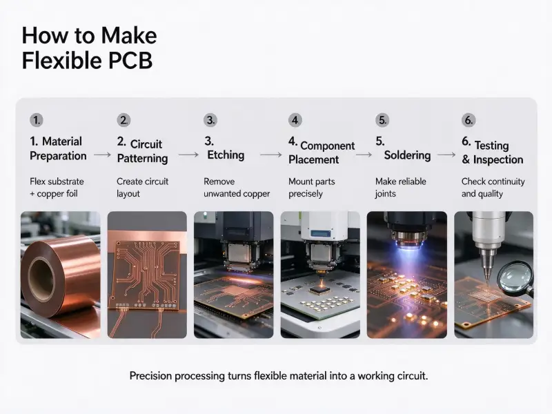
Rigid-Flex PCB Manufacturing Process Overview
Rigid-flex PCB manufacturing follows the same broad sequence as rigid board production but adds a critical lamination step that bonds the flexible and rigid materials, after which the panel is drilled, plated, etched, routed, and tested, with bend and delamination tests applied specifically because of the flex zone.
Lamination and Bonding
The defining step bonds polyimide flex layers to FR-4 rigid layers with prepreg or adhesive under heat and pressure. Controlling prepreg flow is essential so the thin flex core is neither crushed nor starved, and the rigid-to-flex transition must be cleaned and treated so adhesion holds through temperature cycling. Poor bonding at this interface is the most common root cause of field failures.
Drilling, Plating, and Etching
Holes are drilled mechanically or by laser, then plated to connect layers, including the plated transition that carries signals from rigid into flex. Copper is etched into traces routed perpendicular to the bend axis and kept clear of bend and transition zones, and a polyimide coverlay is applied over the flex rather than liquid solder mask.
Testing and Inspection
Beyond standard electrical, optical, and X-ray checks, rigid-flex parts receive mechanical validation. Dynamic bend testing flexes the sample to a specified radius for the required cycle count, thermal shock confirms delamination resistance, and peel-strength checks verify copper-to-polyimide adhesion. These tests, aligned with IPC-6013 for rigid-flex qualification, confirm the board will survive its intended life rather than merely passing a continuity check.

FAQ
What is the minimum bend radius for a rigid-flex PCB?
The minimum bend radius is calculated from the full flex-section thickness and the application type. Per IPC-2223, static bends need roughly 6 times the flex thickness for a single copper layer and about 12 times for two layers, while dynamic bends need 100 times for one layer and up to 200 times for three or more layers. Adding a 20 to 30 percent safety margin is standard practice.
Can rigid-flex PCB thickness be customized for my product?
Yes. Rigid-flex thickness is a design parameter rather than a catalog value. You define the rigid and flex region thicknesses, layer counts, copper weights, and stiffeners to match your enclosure and electrical needs, then confirm a feasible stack-up with the fabricator. There is no universal standard thickness, so customization is the normal way rigid-flex boards are specified.
How do I specify rigid-flex PCB thickness to a manufacturer?
Provide the total layer count for rigid and flex sections, the minimum bend radius and whether the flex is static or dynamic, any controlled-impedance targets, the current-carrying requirements that set copper weight, and the desired finished thickness for each region with its tolerance. Sharing a preliminary stack-up early lets the manufacturer return a buildable proposal and avoid costly redesigns.