+86 18681608727

vebesco@outlook.com

High-Performance Metal Core PCB (MCPCB) Manufacturing

1 – 12 Layers | 1 – 400 W/mK | Al / Cu Core | 99%+ Yield

Request a Quick Quote

ISO 9001:2015

Certified Quality Control

IATF 16949

Automotive QMS

UL 94 V-0

Flame Retardant Base

RoHS & CE

Fully Compliant

100% Hi-Pot

Dielectric Withstand

Metal Core PCB Types by Substrate & Construction

Aluminium Core vs Copper Core vs Hybrid MCPCB

FULL COMPARISON GUIDE (2026 THERMAL SUBSTRATE SELECTION)

KEY PARAMETERS
Aluminium Core
1 – 3 W/mK
Copper Core
~400 W/mK
RECOMMENDED
Hybrid MCPCB
Al + Cu Combined
Base Material
Substrate Composition
Aluminium 5052 / 6061Copper C1100Al + Cu Selective Zones
Thermal Path
Dielectric & Base Conductivity
1 – 3 W/mK(standard thermal prepreg)Up to 400 W/mK(solid copper base)1 – 400 W/mK(zone by zone)
Dielectric Layer
Insulation & Bond Line
50 – 100 µm25 – 75 µmMixed, Per Zone
Thermal Cycling
Long-Term Reliability
Dielectric Fatigue Risk(polymer under 125 °C cycles)Heavier Assembly(mass needs mechanical support)MITIGATEDMetal where it matters
Cost Structure
Material vs. Thermal Budget
Lowest Material Cost(commodity Al core)5 – 8× Al Cost(niche Cu core)Balanced Hybrid CostCu only under hot parts(Al base, Cu inserts)
Primary Applications
Best Use Cases
LED Lighting, Power Supplies, LED DriversRF Amplifiers, HPC, High-Current DriversAutomotive Lamps, Inverters, Power Modules
Source: Electronics Engineering & PCB Manufacturing Standards Guide (2026)DESIGN & SELECTION MATRIX

What is a Metal Core PCB?

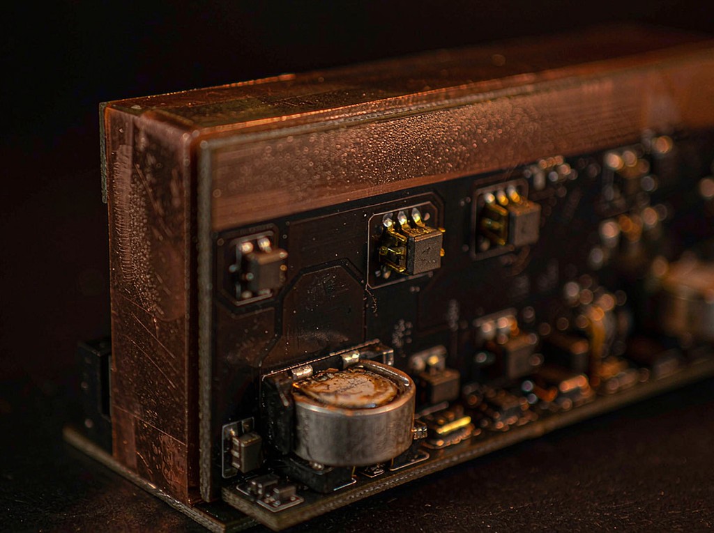
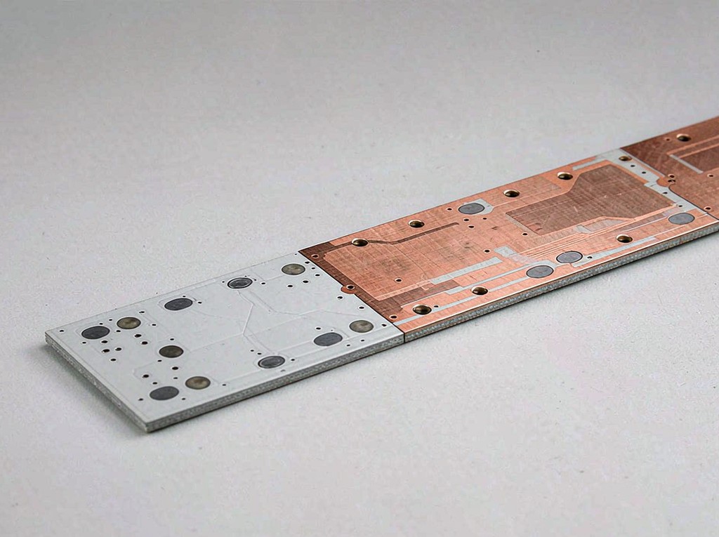
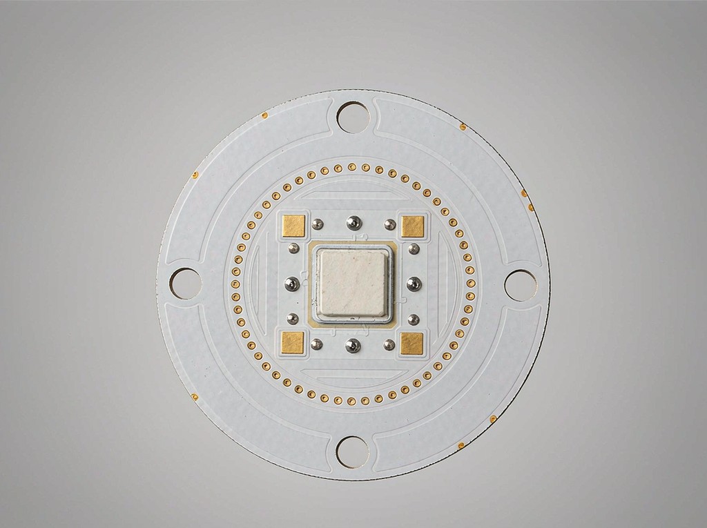
A metal core PCB replaces the fibreglass core of an FR-4 board with a solid aluminium or copper plate. The circuit is bonded to that plate through a thin thermally conductive dielectric, so heat flows from the copper trace straight into the metal instead of being trapped in an insulator.

Key Advantages

  • Heat Dissipation: Transfers heat 5 to 10 times faster than FR-4, dropping junction temperatures and stopping thermal throttling in high-power arrays.

  • Mechanical & Vibration: A solid metal base resists shock, vibration and bending, so heavy transformers and long LED strips need no extra carrier.

  • Lightweight Efficiency: Aluminium delivers most of the thermal benefit at roughly 60% less weight than a solid copper base.

  • Dimensional Stability: Metal cores resist warping and delamination across wide temperature swings, which keeps solder joints intact in outdoor fixtures.

Why Choose Metal Core PCBs

Our lines bond 1 – 4 oz copper to aluminium and copper bases with a 50 – 150 µm thermal dielectric, holding dielectric breakdown above 3 kV and thermal resistance under 1.2 °C/W in volume.

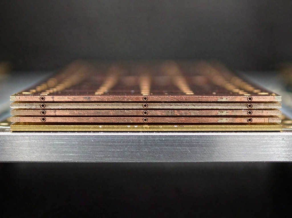
Single-sided LED boards through 12-layer MCPCBs on one thermal line

Aluminium 5052 / 6061 and C1100 copper cores, chosen against your thermal map

Dielectric resistance verified by thermal impedance coupons on every lot

Hi-Pot, AOI and 100% E-test on every panel before packing

Core Advantages

  1. Thermal Design Support: We read your thermal map, then pick aluminium, copper or a hybrid base and set the dielectric thickness so the junction temperature target is met.

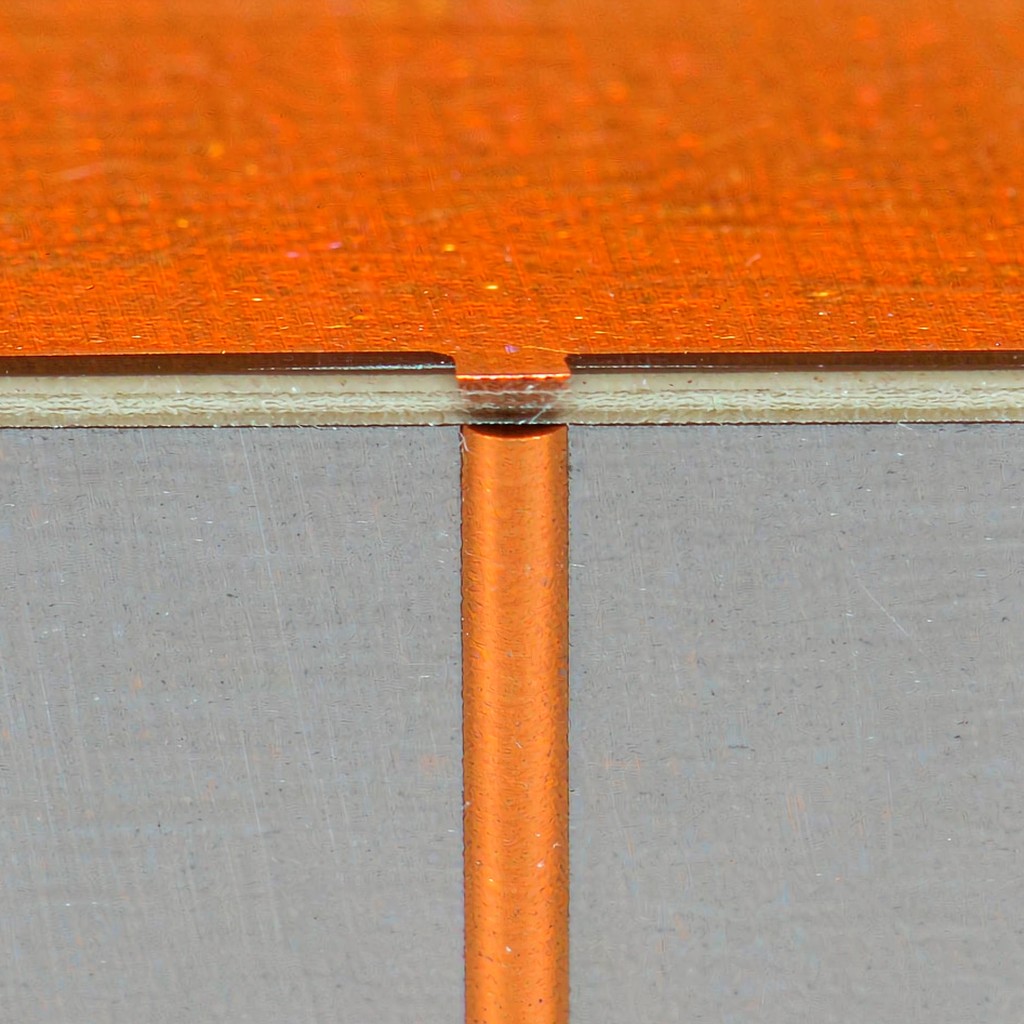
  2. Metal-to-Dielectric Bond: Vacuum lamination and a controlled cure keep the bond line void-free, which is what stops delamination after thermal cycling.

  3. Certified Quality System: ISO 9001 and IATF 16949 processes with Hi-Pot, thermal impedance, AOI and microsection on every lot.

  4. Fabrication + Assembly: Bare MCPCB, LED and power component sourcing and SMT assembly under one roof shorten the program schedule.

Proven Case Study

What is metal core PCB manufacturing?

Metal core PCB manufacturing is the engineering process of bonding an etched copper circuit to an aluminium or copper plate through a thermally conductive dielectric, then drilling, masking and finishing the panel. As an MCPCB manufacturer and trusted metal core PCB supplier, we control dielectric thickness, bond-line voiding and base flatness during the MCPCB fabrication stage so the thermal resistance you simulate is the resistance you receive. By tuning base material and plate thickness for metal core PCBs (also referred to as aluminium PCB boards or MCPCBs), this metal-substrate architecture carries 1 to 12 layers at 1 to 400 W/mK with a 99%+ mass production yield.
Why Choose Slpcba

Built for Thermal Conductivity, Metal Substrates and Repeatable Yield

Al & Cu Substrates

5052 / 6061 aluminium and C1100 copper bases from 0.8 to 3.2 mm thick

1 – 400 W/mK

Dielectric and base chosen against the thermal map, from LED boards to HPC modules

≤ 1.2 °C/W

Bond-line thickness and voiding held by vacuum lamination and coupons

Full-Stage QC

Hi-Pot, thermal impedance, AOI, flying-probe E-test and microsection on every lot.

Ready to Build Your Thermal-Managed MCPCB?

Upload your Gerber files and thermal map today for a free DFM review, a substrate proposal and a detailed quote within 24 hours.

Request a Quick Quote

Upload your Gerber files — DFM review & quote within 24 hours.

Engineering Capability

Technical Specifications & DFM Capabilities

ParameterMetric ValueImperial ValueFeature Highlights
Layer Count1 – 12 Layers1 – 12 LMetal Core Stackup
Thermal Conductivity1 – 400 W/mKAl / CuSubstrate Dependent
Min. Dielectric Thickness0.05 mm2 milLow Thermal Resistance
Min. Trace / Space0.10 mm (4 mil)0.004"Etched Metal Base
Max Metal Base Thickness3.2 mm0.126"Integrated Heatsink
Finished Copper WeightUp to 4 oz (140 µm)Up to 4 ozHeavy Current Traces
Board Thickness1.0 – 4.0 mm±10%Incl. Metal Base

Premium Substrates & Surface Finishes

Surface Treatment Options

✔ HASL (Vertical or Horizontal)

✔ Lead-Free HASL

✔ ENIG (Electroless Nickel Immersion Gold)

✔ ENEPIG (Ni-Pd-Au)

✔ Immersion Silver

✔ Immersion White Tin

✔ OSP (Shikoku F2)

✔ OSP (Entek)

✔ Electrolytic Soft Gold

✔ Electrolytic Hard Gold

✔ Selective Hard Gold

MCPCB Fabrication Tolerances


ParameterMetric ValueImperial Value
Min. Dielectric Thickness0.05 mm0.002″
Max Metal Base Thickness3.2 mm0.126″
Min. Metal Base Thickness0.8 mm0.031″
Min. Mechanical Drill0.20 mm0.008″
Min. Thermal Via0.30 mm0.012″
Min. Trace / Space0.10 mm0.004″
Max Board Thickness4.0 mm0.157″
Thermal Via Aspect Ratio3 : 1Ideal 3:1
Min. Solder Mask Dam0.10 mm0.004″
Max Panel Size520 × 620 mm20.5″ × 24.4″
Material TypeExample / SubtypeFunction
ConductorsHeavy ED Copper (1 – 4 oz)Electro-deposited foil up to 4 oz carries the current on LED and power traces, and still etches to a 4 mil line on the dielectric.
RA Copper (High Reliability)Rolled annealed foil where thermal cycling is severe: its grain structure resists cracking at plated holes in automotive and aerospace builds.
Metal Substrates & DielectricAluminium 5052 / 60611.0 – 3.2 mm plate with 1 – 3 W/mK system conductivity, the cost-effective workhorse for LED and power boards.
Copper C1100Up to 400 W/mK, for extreme heat density in RF amplifiers, HPC and high-current drivers.
Hybrid Al + CuAluminium and copper zones bonded into one panel, so copper sits only where the thermal map needs it.
Thermal Dielectric (50 – 100 µm)Ceramic-filled epoxy that insulates while it conducts heat; its thickness is what sets the thermal resistance.
High-Conductivity DielectricThinner bond line with a high thermal filler, dropping resistance below 1.2 °C/W under power pads.
Base Surface Finishing Anodised or passivated metal side for corrosion resistance and better adhesion in outdoor fixtures.
Insulators & Surface FinishesENIGElectroless nickel with an immersion gold top layer: flat, solderable and stable for fine-pitch LED and driver pads.
Lead-Free HASLHot-air levelled tin-silver-copper finish, the most economical option for through-hole and coarse-pitch MCPCBs.
Immersion SilverSilver finish with excellent solderability for fine lines and press-fit parts, on a flat pad profile.
OSPOrganic solderability preservative: an invisible, flat coating for boards assembled inside a short window.
FAQ

Frequently Asked Questions About Metal Core PCBs

A metal core PCB bonds a copper circuit to a solid aluminium or copper plate through a thermally conductive dielectric. The metal base acts as an integrated heatsink, which is why MCPCBs are standard in high-power LED lighting, power converters, motor drivers, automotive lamps and battery management systems.

Aluminium cores run 1 to 3 W/mK at commodity cost and low weight, which suits LED lighting and power supplies. Copper cores reach about 400 W/mK for extreme heat density such as RF amplifiers, HPC and high-current drivers, at five to eight times the material cost and noticeably more weight.

  • Thinner dielectric: lowers thermal resistance, so heat reaches the base faster, but it also trims breakdown voltage margin.

  • Thicker dielectric: raises isolation and Hi-Pot headroom, at the cost of a higher junction temperature under the same load.

  • Rule of thumb: keep the bond line at 50 to 100 µm on LED boards and confirm the choice with a thermal impedance coupon.

Single-sided (1 layer), double-sided (2 layers) and multilayer MCPCBs up to 12 layers, with blind and buried thermal vias plus custom metal substrate bonds.

Place thermal vias within 5 mm of any heat source above 1 W, keep a 3:1 aspect ratio, and use 0.8 to 1.2 mm diameters under heat-sinking pads. Where the pad must stay flat, fill and cap the vias before masking.

ENIG for fine-pitch driver pads and long storage, immersion silver where solderability and cost both matter, and lead-free HASL for coarse-pitch through-hole work. White reflective solder mask is typical on LED boards because it lifts light output.

4/4 mil (100 µm) line and space, 0.20 mm mechanical drills, 0.30 mm thermal vias and a 50 µm dielectric in volume. Tighter geometry is a development capability, not a standard production specification.

Vacuum lamination with a controlled ramp and cure, an anodised or passivated base, and a bond line held inside 50 to 150 µm. Every lot is screened by thermal cycling and a peel test before shipment.

Yes. Every lot can ship with thermal impedance coupon data, Hi-Pot and dielectric breakdown results, microsection images, plus AOI and flying-probe reports.

Yes. Metal core fabrication, LED and power component sourcing and SMT assembly run under one roof, so a turnkey order arrives tested with one BOM, one freight and one quality gate.

MCPCB thickness is set by the metal base plus the dielectric and copper:

  • Single-sided LED boards: typically 1.0 – 2.0 mm (0.039 – 0.079″);

  • multilayer MCPCBs range from 2.0 – 4.0 mm (0.079 – 0.157″), commonly 2.0 mm (0.079″).

The metal base is cleaned and anodised, the thermal dielectric is laminated or coated on, copper foil is bonded and etched, then the panel is drilled, masked, surface finished, profiled and 100% electrically and Hi-Pot tested before packing.

ISO 9001, IATF 16949, UL 94 V-0 and RoHS. Boards are built to IPC-6012 Class 2 or Class 3 depending on the application, with IPC-2221 rules for clearance and thermal relief.

Key rules: keep thermal vias within5 mm of every heat source above 1 W, hold the dielectric bond line at 50 to 100 µm, keep solder-mask dams above 0.1 mm, and route heavy current on 2 to 4 oz copper so the base spreads heat evenly.

Get Inquiry

Phone/Wechat

+86 18681608727

Email

vebesco@outlook.com

Phone/Wechat

+86 18681608727

Phone/Wechat

+86 18681608727