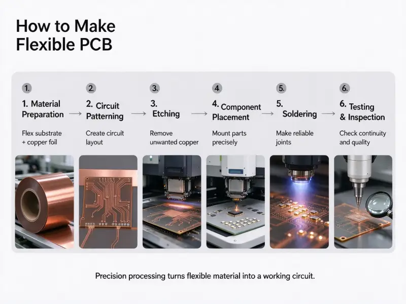
Rigid boards, flex circuits, and rigid-flex boards all connect components electrically. What separates them is the substrate underneath. Rigid boards sit flat in an enclosure and stay there. Flex circuits bend and fold to reach spaces a stiff board cannot enter. Rigid-flex boards combine both in one laminated structure, so rigid sections hold components while flexible sections carry signals across a hinge, a curve, or a fold.
A rigid PCB uses a stiff FR-4 substrate and cannot bend in normal use; a flex PCB uses a thin polyimide substrate and can fold or flex repeatedly; a rigid-flex PCB laminates rigid sections and flexible sections into one continuous board, replacing the connectors and cables that would otherwise join separate boards. Rigid PCBs cover most designs at the lowest cost, flex solves single mechanical bending problems, and rigid-flex solves the case where a product needs rigid component-mounting areas and a flexible interconnect between them at the same time.
The comparison below covers structure, cost, design rules, materials, and manufacturing so you can match the board format to the requirements of your product.

What Is the Difference Between Rigid, Flex, and Rigid-Flex PCBs
The difference comes down to the substrate and whether the finished board can move. Rigid boards use thick glass-fiber laminates that hold their shape and support components anywhere on the surface. Flex circuits use thin polymer films that let the board conform to curved or moving spaces. Rigid-flex boards use both materials in one stackup, so the rigid areas behave like a normal rigid board while the flexible areas act as an integrated ribbon cable.
The structural difference drives nearly every other trade-off. A board that cannot bend is cheap to fabricate but forces designers to split electronics across multiple boards joined by cables. A board that bends freely solves the space problem but cannot support heavy parts without reinforcement. A board that combines both costs more to build but removes connectors from the assembly, which is where many field failures originate. When a product needs rigid mounting area and a flexible connection between separated sections, a rigid-flex PCB manufacturer supplier delivers both in a single part.
| Factor | Rigid PCB | Flex PCB | Rigid-Flex PCB |
| Typical substrate | FR-4 | Polyimide | FR-4 sections plus polyimide sections |
| Bending behavior | Does not bend | Bends and folds repeatedly | Rigid areas fixed, flex areas bend |
| Component mounting | Anywhere on the board | Limited, needs stiffeners for heavy parts | Rigid sections only |
| Fabrication cost | Lowest, well-established process | Higher than rigid for the same circuit | Highest, two processes combined |
| Design complexity | Standard EDA workflow | Requires bend-radius and coverlay rules | Requires rigid stackup rules, flex rules, and transition rules |
| Layer count | High counts supported | Typically 2 to 4 layers | 4 to 6 layers and above with HDI |
| Best-fit use | Flat enclosure, no bend requirement | Ribbon-cable replacement, simple fold or wrap | Multiple rigid zones joined across a hinge or fold |
How each board type is built
A rigid board starts with a cured FR-4 laminate, usually 0.8 mm to 1.6 mm thick, with copper foil bonded on one or both sides, then drilled, plated, and etched.
A flex circuit swaps FR-4 for a polyimide film, often 25 µm to 50 µm thick. Copper is bonded to the film with or without adhesive, and a coverlay film replaces the solder mask a rigid board would use.
A rigid-flex board laminates the two together. Polyimide flex layers run through the stackup, and FR-4 layers are bonded only in the areas that will stay flat, so the board replaces what would otherwise be two or three separate boards plus the cables between them.
Flex PCB vs Rigid-Flex PCB: The Key Difference
A flex PCB is flexible from edge to edge, with no rigid zones unless a stiffener is added. A rigid-flex PCB has defined rigid sections and defined flexible sections in the same laminated board. A flex circuit with a stiffener is not the same thing: the stiffener adds mechanical support to part of the flex, but it does not create an electrical connection through the layers the way a true rigid section does.
This distinction decides how much of the board can carry components. On a plain flex circuit, mounting a connector or a heavy inductor means adding a stiffener underneath that spot, and stiffness is the only thing the stiffener provides. On a rigid-flex board, the rigid section is a full multilayer rigid board bonded into the flex stackup, so it supports connectors, shields, mounting holes, and dense routing.
If the requirement is a single fold or a wrap around one surface, a flex circuit is usually the simpler and cheaper answer. If the product is split into two or more rigid mounting areas joined across a hinge, a curve, or a fold, rigid-flex removes the connectors and cables between them.
Rigid-Flex PCB Stackup and Materials
The stackup sets how the board bends, how signals behave, and how long the part lasts. Review layer arrangement, copper type, and material choices before routing, because the flex layers, the rigid layers, and the transition zones between them all have to be planned together. Changing the stackup after layout is expensive.
A rigid-flex stackup is really two stackups that have to line up. The rigid sections need enough layers to route the dense circuitry and enough copper to carry power. The flex sections need to stay thin, because bend radius scales with total flex thickness. Bonding them requires no-flow prepreg, which keeps resin from flowing into the flex areas during lamination.
Common stackup options
| Stackup | Typical use | What to check |
| 1 or 2 flex layers | Wearables, displays, sensor leads, small controllers | Bend radius, coverlay, connector support |
| 4-layer rigid-flex | Medical handhelds, compact sensors, IoT devices | Plane continuity, impedance limits |
| 6-layer or HDI rigid-flex | Camera modules, RF devices, dense electronics | Lamination cycles, microvias, bend life, yield |
Symmetry carries more weight in a rigid-flex stackup than in a plain rigid board. If copper layers and dielectric thicknesses are unbalanced across the neutral axis, the board can warp or twist during reflow, and the flex sections may pull out of alignment. The stackup is also a good place to start when planning a project with a flexible PCB supplier custom FPC.
Material choices
The two material systems in a rigid-flex board behave differently, and the interface between them is where problems start.
- Flex layers: Polyimide film is the default substrate for the flexible areas. It handles heat and repeated bending better than polyester.
- Rigid layers: FR-4 remains the standard for rigid sections. High-Tg laminates are often chosen when the assembly will see elevated temperatures.
- Copper: Rolled annealed copper resists fatigue better than electrodeposited copper and is preferred for dynamic bending areas.
- Bonding: Adhesiveless laminates reduce stackup thickness, which helps bend radius, but they usually cost more.
- Prepreg: No-flow prepreg keeps resin out of the flex areas during lamination.
Two standards set the common expectations for these choices. IPC-2223 covers design requirements for flexible printed circuits, and IPC-6013 covers qualification and performance requirements for rigid-flex boards.

Rigid-Flex PCB Design Guidelines
Most rigid-flex failures trace back to three places: the flexible sections, the bend lines, and the transition zones where rigid and flexible materials meet. Treat each as a keep-out area for parts, vias, and abrupt geometry changes, and the design will hold up far better under bending and thermal cycling. The guidelines below are starting points, not final specifications.
Bend radius and flex area rules
| Flex condition | Starting bend radius | Notes |
| Single-layer static bend | About 6x to 10x flex thickness | Fine for a one-time assembly fold |
| Double-layer static bend | About 10x to 15x flex thickness | Check copper stress and neutral axis |
| Dynamic bend | Often 20x to 40x flex thickness or more | Confirm with bend-cycle testing |
A static flex section is bent once during assembly and stays in that position. A dynamic section moves repeatedly during normal use, such as a hinge that opens thousands of times. Dynamic sections need the larger radius, thinner copper, fewer flex layers, and a defined flex-cycle life target agreed with the fabricator. Applying static-flex margins to a dynamic application is a common cause of field cracking.
Inside the flexible area, the layout rules are restrictive for good reason:
- Do not place components, vias, test pads, solder joints, or plated holes in the bend zone.
- Route traces parallel to the bend axis so the copper flexes along its length rather than across it.
- Avoid sharp 90-degree corners; use curved traces or gentle angles.
- Avoid abrupt trace width changes, which concentrate mechanical stress.
- Offset traces on different layers instead of stacking them directly.
Rigid-to-flex transition and component placement
The transition where a rigid section meets a flex section is the most stressed part of the board. A common starting point is a clearance of about 2 mm around it, widened slightly for dynamic applications, with vias and plated holes kept clear of the zone.
Component placement follows the same logic. Keep surface-mount parts at least 1.5 mm away from the transition so bending stress does not transfer into solder joints. Restrict heavy parts, roughly 1 g and above, to the rigid sections. Put heat-generating parts on the rigid sections with enough copper to spread heat, since the thin flex substrate dissipates heat poorly.
The 3W rule and trace spacing
The 3W rule is a spacing guideline for reducing crosstalk between adjacent traces. It states that the center-to-center distance between two parallel signal traces should be at least three times the trace width. For a 4 mil trace, that means 12 mil center-to-center, or about 8 mil edge to edge.
Crosstalk comes from parasitic capacitance and mutual inductance between nearby traces. Increasing the distance cuts the coupling, and the effect is steep: roughly 3W spacing isolates about 70% of the electric field interference, while 10W spacing pushes the reduction toward 98%. The rule matters most on sensitive nets such as high-frequency clocks, high-speed data buses, differential pairs, and video or audio lines.
The rule is a starting point, not a fixed requirement. It assumes a 50-ohm characteristic impedance and depends on the stackup. On a four-layer board with the signal layer 5 to 10 mil above a reference plane, 3W is generally enough. On a two-layer board where that distance runs 45 to 55 mil, 3W may not be sufficient.
Rigid-Flex PCB Manufacturing Process
Rigid-flex manufacturing is harder than either rigid or flex manufacturing because it combines both. Rigid and flexible layers are laminated in multiple cycles, and the two materials expand at different rates under heat. That mismatch, plus the handling demands of thin flex panels, drives the process complexity and the yield risk.
Fabrication steps
- Inner layer imaging. Rigid and flexible inner layers are patterned separately. Flex layers may need different etch tolerances because the copper is thinner.
- Stackup and layup. Flex cores and rigid layers are aligned with no-flow prepreg in the flex areas. Misalignment here shows up later as impedance variation or shorts.
- Multiple lamination cycles. Rigid sections are bonded in more than one press cycle so the flex areas stay free of resin. Each cycle adds handling risk to the thin flex material.
- Drilling, plating, and outline. Vias may cross from rigid into flex layers, and plating adhesion on polyimide is weaker than on FR-4. The flex areas then receive a coverlay instead of a solder mask.
- Test and inspection. Flex areas are checked for tears and the transitions for delamination, in addition to the standard electrical test.
The material mismatch between FR-4 and polyimide is the central difficulty. The two expand at different rates as the board heats and cools, and that difference concentrates stress at the transition zones.
Testing and quality control
Rigid-flex boards often go into products where field failure is expensive, so testing tends to be more rigorous than for a standard rigid board. Qualification may include bend-cycle testing on the flex sections, thermal shock to check the transitions, and electrical tests on every net. Critical applications may call for IPC Class 3 requirements.
Rigid-Flex PCB Cost and Total System Cost
A rigid-flex board costs more per square inch than a rigid board, often by a wide margin in low volumes. The gap narrows or reverses at the system level when the rigid-flex part replaces connectors, cables, and the assembly labor that would have joined separate boards. Whether rigid-flex is the cheaper option depends on the whole product, not the board alone.
What drives the price
Four things push a rigid-flex quote above a rigid board quote. Polyimide film and adhesiveless construction cost more than FR-4 laminate. Lamination runs through multiple press cycles, which adds labor, tooling, and scrap risk. Flex circuits often run on smaller panels with more waste, so material utilization is worse. And every added feature, from stiffeners to shielding films to pressure-sensitive adhesives, adds material and assembly steps.
Volume changes the picture. Rigid boards benefit from decades of process maturity and large panel sizes, so their cost drops quickly with quantity. Flex and rigid-flex production runs on smaller panels with more manual handling, and the economies of scale are weaker. Thin flex handling and transition lamination also hold yields below what a rigid shop achieves.
Where rigid-flex saves money
The savings sit outside the board price. A rigid-flex section that replaces a connector, a wiring harness, and the labor to assemble them removes several line items from the bill of materials at once. It also removes the crimps and connector mating interfaces that account for a large share of field failures in products that flex or vibrate.
There is no standard ratio that says when the system savings win. The crossover depends on the connector count you remove, the assembly steps you eliminate, the harness cost, and your expected return rate. A supplier comparing options honestly should run that calculation against your project data rather than quoting a rule of thumb.
When to Choose Each Board Type
Default to a rigid PCB unless there is a specific mechanical requirement that demands otherwise. Choose flex when the circuit has to bend or fold to fit a non-flat or moving space. Choose rigid-flex when the product needs rigid component-mounting areas joined by a flexible interconnect across a hinge, curve, or fold.
| Question | If yes | If no |
| Does the circuit need to bend during assembly or use? | Consider flex or rigid-flex | Rigid is likely sufficient |
| Are electronics split across two or more flat areas joined by a hinge or fold? | Consider rigid-flex | Rigid may work |
| Is connector or cable failure a known reliability concern? | Rigid-flex removes those interfaces | Rigid with connectors may be fine |
| Is the product exposed to continuous vibration or repeated motion? | Rigid-flex or flex with proper strain relief | Rigid is generally adequate |
| Is volume high and cost the primary constraint? | Rigid, unless bending is unavoidable | Rigid-flex becomes more viable at lower volume |
Repair and rework favor rigid boards, because a failed component can be replaced with standard tools, while flex and rigid-flex assemblies are harder to rework without damaging the substrate. Lead time also matters: rigid fabrication is widely available, while flex and rigid-flex require specialized processes and a smaller supplier base.
FAQ
Can rigid-flex PCBs handle high layer counts and HDI features?
Yes, with limits. A 4-layer rigid-flex stackup is common for medical handhelds and IoT devices, and 6-layer or HDI constructions show up in camera modules and dense RF products. Microvias of about 0.15 mm or less are used in high-density flex areas. Flex sections stay thin for bendability, so layer count is usually lower there than in the rigid sections, and each added lamination cycle raises the yield risk. Plan the layer count around the bend requirement, not the other way around.
What bend radius should I specify for a dynamic flex section?
Start at 20 times the total flex thickness and treat it as a floor, not a target. Some designs need more, depending on copper type, layer count, and the number of bend cycles the part must survive. Rolled annealed copper and a thinner flex stackup both allow a tighter radius for the same life. Since dynamic flex failure is a fatigue problem, the radius should be confirmed with bend-cycle testing at the expected life.
Does replacing a connector with a rigid-flex section change reliability testing?
A connector-based design concentrates testing on the mating interface, the crimp, and the strain relief. A rigid-flex design shifts that focus to the flex sections and the rigid-to-flex transitions, where bend cycles, delamination, and copper fatigue are the failure modes of concern. The net effect is often fewer interfaces to qualify for, but more testing per interface that remains.