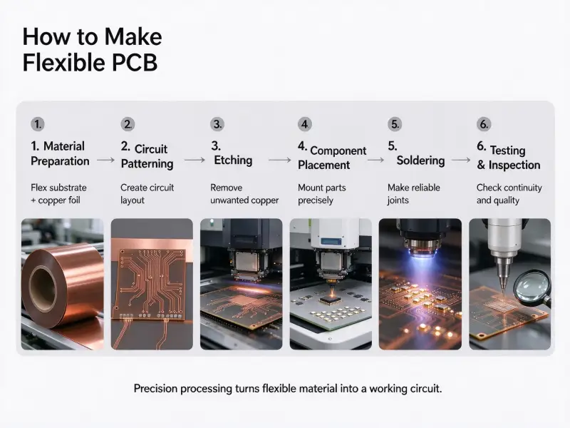
Rigid-flex PCBs solve a specific problem: a product needs a board that holds components steady in one area and bends in another, without a cable or connector bridging the two. Medical catheters, avionics racks, and folding consumer devices all run into this. The usual workaround is a rigid board plus a wire harness, which adds a connector, a solder joint, and a mechanical failure point for every transition. Rigid-flex technology removes those transitions by building the rigid and flexible sections as one continuous board.
The advantages of rigid-flex PCBs come from removing hardware rather than adding it: fewer connectors and cables mean less weight, less volume, fewer failure points, and shorter assembly time. The challenges come from the same source. A board that bends must survive that bending, which forces tighter rules on bend radius, stackup, material choice, and the transition zone where rigid meets flex. Most rigid-flex projects fail on design discipline, not on fabrication capability.
The sections below walk through what rigid-flex is, where it wins, where it costs more, and how to design and qualify it without surprises.

What Is a Rigid-Flex PCB?
A rigid-flex PCB is a single circuit board built with both rigid and flexible sections. The rigid areas carry components and provide mechanical support; the flexible areas bend or fold to connect them. The flexible regions are typically built from polyimide film and laminated into the rigid stack during fabrication, so the board arrives as one piece rather than as separate boards joined by cables.
The flexible region is not a general-purpose bending zone. It is a defined area where the stackup changes: the rigid laminations and stiffeners stop, the coverlay replaces the solder mask, and the copper type often changes from electro-deposited to rolled annealed. Everything about that area is a design decision, and it is where most of the technical risk lives. A qualified rigid-flex PCB manufacturer supplier reviews the flex zone and transition geometry before quoting, because those two features drive both yield and cost.
Rigid-flex vs. flex PCB: what actually changes
The two are often treated as interchangeable, but they are different constructions with different design rules.
| Feature | Rigid PCB | Flex PCB | Rigid-flex PCB |
|---|---|---|---|
| Bending | Not designed to bend | Entire board can bend | Only defined flex zones bend |
| Component support | Rigid substrate everywhere | Requires stiffeners for component areas | Rigid sections built in |
| Connectors and cables | Needed to join boards | Usually needed | Largely eliminated |
| Stackup complexity | Standard multilayer | Flex-only lamination | Hybrid: rigid and flex laminated together |
| Design rules | Baseline IPC rigid rules | Flex rules throughout | Rigid rules plus flex rules plus transition rules |
| Typical cost | Lowest | Moderate | Highest |
The practical difference: on a flex PCB, every square millimeter must be designed to survive bending, which limits where you can place components and how you route. On a rigid-flex board, bending is confined to zones you choose. That makes component placement and routing simpler in the rigid areas while keeping the flex benefit where it matters.
Where rigid-flex fits in a product
Rigid-flex earns its cost when three conditions overlap: the enclosure is space-constrained, weight matters, and the assembly has to survive vibration, shock, or repeated motion. Miss any one of those and a rigid board with a cable is usually the better buy.
Common applications follow the same logic:
- Medical devices. Catheter tips, endoscopic controllers, and implantable assemblies need a board thin enough to pass through narrow channels and reliable enough to tolerate handling and sterilization. Dynamic bending cycles at the tip are the design constraint.
- Aerospace and defense. Avionics weight reduction compounds across an airframe, and connector count directly affects reliability in high-vibration environments.
- Automotive. Camera modules, sensor packages, and dashboard assemblies fold into shapes that a flat rigid board will not fit.
- Industrial and wearables. Compact sensor nodes and body-worn devices need a board that conforms to a curved shell and survives constant flexing.
In each case the driver is the same: the product cannot be assembled from rigid boards and cables, or cannot be assembled affordably that way.
Advantages of Rigid-Flex PCBs
Rigid-flex boards win by eliminating parts. Every connector, cable, and solder joint removed is a component that no longer needs to be sourced, placed, inspected, or protected from vibration. The gains show up as smaller volume, lighter assemblies, higher reliability, and simpler assembly, often outweighing the higher cost of the bare board itself.
Space and weight savings
The space argument is usually what starts the conversation. A rigid-flex design removes the connectors and harnesses that would otherwise bridge separate boards, so the enclosure no longer needs room for those parts or for the bends and service loops that cables require.
A flex zone can also be folded into a three-dimensional shape, which lets a single board follow the inside of a curved or stepped enclosure. Designs that previously needed two or three rigid boards can collapse into one. Weight follows volume: fewer connectors, less cable, and less board area add up, which matters most in drones, wearables, and anything battery-limited where every gram affects runtime.
Reliability gains from fewer interconnects
Connectors and cable terminations are a leading source of field failures. They work loose under vibration, corrode, and fatigue at the crimp or solder joint. Rigid-flex eliminates most of them by making the connection a continuous etched trace instead of a mechanical joint.
That is why rigid-flex shows up in high-vibration environments. Fewer mechanical interfaces mean fewer things to shake apart. The trade-off is that the remaining interfaces, especially the rigid-to-flex transition, become the critical ones and need proper design and inspection. Reliability is not automatic; it comes from concentrating effort on a smaller number of features.
Assembly and cost implications downstream
A single rigid-flex board replaces what would otherwise be a multi-board assembly with interconnecting hardware. That reduces the bill of materials, the number of placement steps, the number of solder joints, and the labor required to assemble and test the unit.
The savings are real, but they land downstream, in assembly, not upstream in fabrication. The bare rigid-flex board costs more to make than an equivalent rigid board. Whether the total project cost falls depends on how much hardware the design removes, and that calculation has to be done per project rather than assumed.
Challenges in Rigid-Flex PCB Design
The challenges in rigid-flex design all trace back to the flex zone. A rigid board can be designed and fabricated almost independently; a rigid-flex board has to be designed as a mechanical part and an electrical part at the same time. Bend radius, stackup, material compatibility, and the transition zone all have to be correct together, because a finished rigid-flex board that fails mechanically cannot be fixed by rework.
Bend radius and mechanical limits
Bend radius is the minimum curvature radius a flex zone can be formed to without damage. Go below it, and the copper traces crack, the coverlay lifts, or the layers delaminate. The failure may not show up at fabrication; it appears after installation or after some number of flex cycles.
The rule of thumb is that bend radius scales with flex thickness, and the multiplier depends on construction and whether the bend is static (formed once during assembly) or dynamic (repeated during operation). Dynamic bends need a considerably larger radius than static bends of the same thickness. Keep the flex zone as thin as the design allows, and route conductors perpendicular to the bend line so the copper grain structure works with the bend rather than against it.
Stackup and material matching
A rigid-flex stackup is not symmetric in the usual sense, because the flex zone has fewer layers than the rigid zone. The two materials also expand differently with temperature. Rigid laminates and polyimide flex films have different coefficients of thermal expansion, so as the board heats during assembly and in service, the two sections move by different amounts.
That mismatch concentrates stress at the transition. If the design does not account for it, the result is cracked plated barrels, delamination, or intermittent opens after thermal cycling. Material selection and stackup symmetry around the neutral axis both matter here, which is why the flex zone layout and the material set should be decided together rather than sequentially.
Signal integrity, EMI, and thermal management
Controlling impedance is harder in a flex zone. The dielectric thickness and the geometry around a conductor shift as the board bends, and a trace that meets its target impedance flat may drift when the zone is formed. High-speed signals crossing a flex zone need controlled-impedance design plus verification on the finished board, not just on the design files.
EMI is related, since the flex region has less reference plane coverage than a rigid multilayer section. Thermal management adds another constraint: polyimide is a poorer conductor of heat than a rigid laminate backed by copper planes, and the flex zone has less copper to spread heat. Heat-generating components should stay on the rigid sections, close to thermal vias or plane copper.
Design rules and verification
The design rule set for a rigid-flex board is larger than for a rigid board. It includes the rigid rules, the flex rules, and a set of transition rules covering where stiffeners stop, how coverlay terminates, which layers may place vias near the flex boundary, and how much resin flow is acceptable. Missing any of these produces a board that passes electrical tests and fails mechanically.
Verification is harder too. A rigid-flex board is three-dimensional, so visual inspection of the flex zone and the transition is limited. Microsection, impedance testing, and dynamic applications like bend-cycle testing become part of the qualification package rather than optional checks. That adds cost and lead time, and it needs to be planned into the project schedule from the start.
Rigid-Flex PCB Stackup and Material Selection
A rigid-flex stackup is built from three regions: the rigid sections, the flex sections, and the transition between them. The rigid sections use standard laminate, prepreg, and copper; the flex sections use polyimide film with rolled annealed copper and a coverlay instead of solder mask; and the transition is where the rigid laminations end and the flex layers continue through. Stackup and material choices determine how many flex cycles the board can take and how well it survives assembly.
How a rigid-flex stackup is built
The construction starts with the flex core. One or more polyimide layers are laminated with copper and covered with a polyimide coverlay on both sides, leaving the flex zone free of rigid material. The rigid sections are then built up on either side of the flex core using prepreg and rigid laminate, with no-flow prepreg at the transition so resin does not flow into the bend area.
The result is an asymmetric structure by design. The flex zone may be a fraction of the total layer count in the rigid sections. Layer counts for hybrid constructions commonly run from a few layers up to twenty or more depending on the application, and the flex zone itself is usually limited to a smaller number of conductive layers to keep it thin enough to bend.
Stiffeners, made from polyimide, FR-4, or metal, are added where components need extra support or where the flex zone needs to be held flat at a connector. Their placement is part of the stackup decision, not an afterthought.
Base materials, copper, and adhesives
Material selection in the flex zone comes down to a few choices that directly affect bend life.
| Material choice | Option | Where it fits |
|---|---|---|
| Base film | Polyimide | Standard flex dielectric; high temperature and good dimensional stability |
| Base film | Polyester (PET) | Lower-cost flex for static or lightly flexed applications |
| Copper | Rolled annealed (RA) | Dynamic flex zones; grain structure aligned with the bend axis, higher ductility |
| Copper | Electro-deposited (ED) | Rigid sections and static flex zones; better fine-line definition, lower flex fatigue life |
| Base construction | Adhesiveless | Improved flexibility, lower Z-axis expansion, less moisture absorption |
| Base construction | Adhesive-based | Lower material cost; the adhesive layer adds thickness and can affect flex life |
| Coverlay | Polyimide with acrylic or epoxy adhesive | Protects flex conductors in place of solder mask |
| Rigid laminate | FR-4 or equivalent | Rigid sections; mechanical support and component mounting |
Two choices drive most of the reliability difference. First, copper type: rolled annealed copper has a grain structure that tolerates repeated bending far better than electro-deposited copper, so dynamic flex zones should specify it. Second, adhesiveless construction: casting polyimide directly onto copper removes the adhesive layer, which reduces Z-axis expansion and moisture uptake and improves long-term flex performance. Both choices raise material cost, and both are worth it in zones that will actually move.
Rigid-Flex PCB Design Guidelines
The design guidelines for a rigid-flex board follow from the challenges: keep the flex zone as simple and as thin as possible, route it so the copper is not asked to do more than it can, and treat the transition as a critical feature with its own rules. These are rules you apply at layout, not problems you can inspect your way out of later.
Rules for the flex zone
The flex zone should be as thin as the electrical requirements allow, since bend radius scales with thickness. Beyond that:
- Route conductors perpendicular to the bend line. A trace running across the bend is asked to stretch and compress along its width; a trace running along the bend axis only bends. Where a flex zone must bend in two directions, plan the routing and the bend locations together.
- Keep the copper balanced. Use a crosshatched or uniform copper pattern in the flex zone rather than large solid pours. Balanced copper distributes stress and prevents one layer from dominating the bend.
- Define a keepout around the bend. No vias, no plated through holes, no component pads, and no stiffeners in the bend area. A plated hole in a bend region is a crack waiting to happen.
- Route conductors on the neutral axis where possible. Placing the critical signal layer at the mechanical center of the flex stack reduces the strain it sees.
- Add tear guards and stress relief. Rounded flex-zone outlines and fillets where the flex enters the rigid section reduce stress concentration at the corners.
On the question of vias in flex circuits: they are possible, but their placement is constrained. Plated vias in a flex zone are acceptable only outside the bend region, and they need adequate annular ring and plating quality. In the bend region itself, vias should be avoided entirely. This is one of the reasons the rigid zones carry the routing density and the flex zone stays a relatively simple interconnect.
Routing across the rigid-to-flex transition
The transition zone is the highest-risk area on a rigid-flex board. It is where the stiff, rigid stack meets the thin, flexible stack, and where mechanical stress concentrates.
- Keep the transition short and well defined. A clean, narrow boundary between rigid and flex gives the mechanical stress a defined place to act and makes it easier to control resin flow.
- Maintain impedance through the transition. Conductor geometry changes as the stack changes, so impedance can shift across the boundary. Verify it on the finished board rather than assuming the design carries through.
- Control resin flow. Use no-flow prepreg at the transition and specify the acceptable flow limits. Resin that squeezes into the flex zone stiffens it and seeds cracks.
- Do not place vias close to the boundary. Plated through holes near the rigid-to-flex edge are exposed to concentrated stress. Keep them back from the transition by the margin the design rules and the performance class require.
- Size stiffeners and coverlay terminations deliberately. Stiffeners should end cleanly and away from the bend; coverlay should terminate within the flex zone where it can bond fully.
What Drives Rigid-Flex PCB Cost
Rigid-flex PCB cost comes mainly from materials and process complexity, not from the board area. Adhesiveless polyimide, rolled annealed copper, and no-flow prepreg all cost more than their rigid-board equivalents. Add the extra lamination steps, the lower yield on complex stackups, and the inspection and test evidence that rigid-flex requires, and the bare board price rises well above a comparable rigid board. The savings appear later, in assembly.
Where the cost comes from
| Cost driver | Effect |
|---|---|
| Base material | Polyimide and adhesiveless construction cost more than FR-4 and adhesive-based flex |
| Copper type | Rolled annealed copper costs more than electro-deposited |
| Layer count and stackup complexity | More layers, more lamination cycles, and asymmetric hybrid stackups lower yield |
| Flex zone count and geometry | Multiple flex zones and tight bend radii increase process difficulty |
| Stiffeners and coverlay | Additional materials and placement steps |
| Performance class | Higher classes require more inspection, microsection, and test evidence |
| Flex cycle requirement | Dynamic applications require bend testing and often higher-grade materials |
| Volume | Rigid-flex has a steeper learning curve per design, so low volumes carry more setup cost |
The last item matters for budgeting. Rigid-flex is a design-specific process: each new stackup has to be proven, which is why the first build of a new design costs more than the tenth. This is also why rigid-flex tends to be an expensive prototyping choice, even when the production economics work.
When the higher unit cost is justified
A higher board price is not the same as a higher project cost. Rigid-flex earns its place when the removed hardware and assembly steps outweigh the board premium:
- The design would otherwise need multiple boards, connectors, and cable assemblies.
- Assembly labor and test time are a significant share of unit cost.
- The unit ships into a high-vibration or high-reliability environment where a connector failure is expensive to service.
- The enclosure physically cannot accommodate rigid boards and cables.
Rigid-flex is usually the wrong choice when the product is a flat, stationary board that fits its enclosure, when volumes are high and the design is already cost-optimized as rigid, or when the bend requirement is a one-time installation fold that a simple cable could serve. In those cases the premium buys nothing.

Rigid-Flex PCB Manufacturing and Qualification
Rigid-flex PCB manufacturing is a lamination process first and a circuit process second. The fabrication house must be able to build rigid and flex sections as one piece, hold registration through multiple lamination cycles, and control resin flow at the transition. Qualification rests on the IPC standards that define construction types, performance classes, and acceptance criteria, and on the test evidence produced against them.
What to specify on the fabrication drawing
A rigid-flex drawing that leaves the key fields blank forces the fabricator to guess, and guessing on a hybrid stackup is how disputes start. The drawing should state:
- The governing standard and its revision. For flex and rigid-flex boards, IPC-6013 is the qualification and performance specification. The IPC-6013 qualification and performance specification for flexible and rigid-flexible printed boards separates the field into construction types and performance classes, and it is the document a quality team inspects against.
- The construction type. IPC-6013 classifies flex and rigid-flex boards by construction, from single-sided flex up through multilayer rigid-flex with plated through holes. Construction type describes the build, not the quality level.
- The performance class. Class 1, 2, and 3 set progressively tighter acceptance limits, more microsection evidence, and stricter release gates. Class 3 suits high-reliability work such as aerospace, military, and medical; applying it to the whole board when only the transition needs it adds cost without benefit.
- The installation and use category. This field drives copper type and coverlay selection, and it is the one most often left off drawings. For applications with repeated flexing, the required number of flex cycles has to be stated, or there is nothing to test against.
- Design rules referenced. Bend radius and flex-zone layout rules belong to the design standard for flex and rigid-flex boards, not the performance standard. Cite both, or the design intent is not fully specified.
Providing Gerber files with an explicit layer stackup and clearly defined flex zones saves a revision cycle. Copper weight, surface finish, and stiffener specifications round out the package.
Inspection and test evidence
Three features carry most of the rigid-flex risk, and each has its own acceptance criteria:
- The transition zone. Inspect for resin or adhesive flow into the bend, coverlay registration and adhesion at the boundary, and a clean, void-free bondline confirmed by microsection on qualification or first-article lots.
- The bend region. The flex zone should be clean and balanced, with no adhesive squeeze-out, the correct copper type, and keepouts respected.
- Plated interconnect. Plating thickness, copper wrap, and barrel integrity at the flex-to-rigid junction are verified by microsection. These criteria are what separate one performance class from another.
For dynamic applications, bend-cycle testing is performed at the specified radius and cycle count while monitoring continuity, with a defined resistance increase counting as failure. Impedance testing on finished boards verifies that the controlled-impedance design survived lamination. Flexible PCB supplier custom FPC can produce flex and rigid-flex constructions in-house, which can often shorten this loop, since stackup questions are resolved during design review rather than after a failed build.
FAQ
Do flex PCBs need vias to be plated differently?
Plated vias in a flex or rigid-flex board are built to the same quality requirements as rigid vias, but the constraints around them differ. Vias must stay out of the bend region, need an adequate annular ring to survive mechanical and thermal stress, and are inspected for barrel integrity by microsection. In dynamic flex applications, the plating quality at vias and the plated barrels near the transition zone are among the first features to fail, so they get closer inspection than they would on a rigid board.
Can a rigid-flex PCB be repaired after the flex zone cracks?
Rarely in a way that restores reliability. A cracked conductor in the flex zone is usually a symptom of a bend radius or material problem that affects the whole zone, not an isolated defect. Local repair, such as a jumper or a reflowed joint, can restore continuity but leaves the mechanical cause in place. In high-reliability applications, the standard approach is to treat the board as unserviceable and correct the design or the assembly process. Small defects in the rigid sections are more often repairable.
Is rigid-flex worth it for low-volume production?
It can be, if the alternative is a multi-board assembly with connectors and cables, because the savings come from assembly and hardware rather than from board volume. The catch is that each new rigid-flex stackup carries a setup and qualification cost, so the first build is disproportionately expensive. At low volumes, the decision usually comes down to whether the product physically requires rigid-flex. If it does, volume is not the deciding factor.