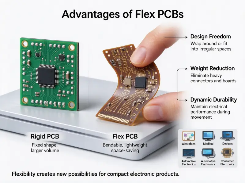
Devices keep getting smaller, lighter, and harder to package. As enclosures shrink, linking several separate rigid boards with cables and connectors eats space and adds failure points that vibration and time eventually expose. A rigid-flex PCB answers that by building rigid and flexible circuitry into a single board. Sourcing the part from a rigid-flex PCB manufacturer supplier that runs both rigid and flex processes under one roof keeps the rigid-to-flex transition in a single accountable build.
A rigid-flex PCB is a hybrid printed circuit board that combines rigid sections and flexible sections in one continuous unit. The rigid areas carry components and connectors, while the flexible areas fold and bend to link those sections, removing separate cables and many of the connectors that normally join multiple boards.
The sections below explain what the board is made of, how it is stacked and built, what the design rules demand, and where it pays off.
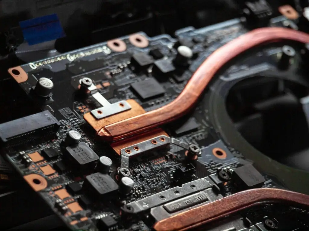
The three main types of PCBs
Rigid, flex, and rigid-flex PCBs differ in whether they bend and how many circuit regions they carry: rigid boards stay fixed, flex boards bend, and rigid-flex boards join both in a single part.
Most designs start from one of three board families, and the choice shapes everything downstream, from layout tools to assembly fixtures.
Rigid PCBs
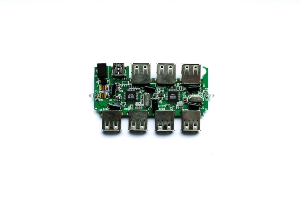
A rigid PCB is the familiar flat board that does not bend. It is built from a solid substrate such as FR-4 and works well for standard shapes and high-volume runs. It is cheap to make in bulk and easy to assemble, but it cannot conform to a curved or folding enclosure, so it relies on cables to reach boards in other parts of the product.
Flexible PCBs
A flexible PCB, often called an FPC, uses a thin dielectric such as polyimide with etched copper on top. It bends and folds to fit tight spaces and saves weight, which matters in wearables and portable gear. On its own, though, it is harder to populate with heavy components and more awkward to handle during assembly, since the thin film wants to curl.
Rigid-flex PCBs
A rigid-flex PCB merges the two. Rigid islands hold the components and connectors, and flexible tails route signals between them. The result is one part that folds into a three-dimensional shape instead of a stack of boards joined by wires, which is why it shows up in products where every millimeter counts.
| Board type | Bends? | Best for | Main limit |
|---|---|---|---|
| Rigid PCB | No | High-volume, standard enclosures | Cannot conform to shape |
| Flexible PCB | Yes | Tight, light, moving spaces | Weak for heavy parts, awkward assembly |
| Rigid-flex PCB | Partial (flex zones) | 3D packages, high reliability | Higher design and build cost |
What a rigid-flex PCB is and how it works
A rigid-flex PCB works by burying flexible circuit layers inside a rigid laminate so rigid regions stay stable while flexible regions carry interconnections that bend or fold.
The board is not two parts glued together after the fact. The rigid and flexible materials are stacked and bonded as one assembly, so the electrical path never passes through a discrete connector between the two zones. Components mount on the rigid areas, and the flexible layers run underneath to connect those areas without separate wires.
Core construction and buried flex layers
In a typical build, the flexible layers pass through the rigid sections and terminate at plated holes that join them electrically to the rigid copper. Drilling and plating create the through-connections, and imaging and etching form the copper pattern on each layer. A coverlay or flexible solder mask then protects the circuitry from moisture and abrasion. Because the flex layers are buried, the finished board reads as rigid where it needs to be and bends only where the layout allows, which is what gives it the folded final shape.
Rigid-flex PCB materials
Rigid-flex PCB materials must be picked in pairs so the rigid and flexible sections survive temperature changes together, which makes material selection one of the first design calls.
The two zones use different substrates, and their coefficients of thermal expansion have to stay close enough to avoid cracking at the joints when the product heats and cools.
Rigid section substrates
The rigid areas commonly use FR-4 for cost-sensitive layers and higher-performance laminates such as polytetrafluoroethylene-based materials where frequency or loss matters. The choice depends on signal speed and the environment, not on a single default, so a board may mix a standard rigid layer with a premium RF layer only where the circuit needs it.
Flexible substrates and copper
The flexible sections rely on polyimide film or polyester for lower-cost uses. Copper is laminated onto the film, and the grade matters: rolled-annealed copper bends far better than electrolytic copper, so dynamic flex zones usually call for the rolled type. The adhesive that bonds the film to copper also has its own expansion behavior, and matching it to the polyimide keeps the flex tail from lifting at the edges.
Covers and stiffeners
A coverlay, not a standard liquid solder mask, protects the flex circuitry because it bends with the film instead of cracking. Stiffeners such as polyimide or aluminum sheets add local support under connectors or component pads without making the whole board rigid, so a thin tail can still carry a bulky connector.
Rigid-flex PCB stackup
A rigid-flex PCB stackup alternates rigid and flexible layers and bonds them with adhesive so the flexible portions stay continuous through the rigid blocks.
Stackup is where the board takes its final form. A simple part might pair one double-sided flex zone with two rigid sections, while a complex part stacks many layers with several flex branches reaching different corners of the product.
The flexible layers are often left unbonded in the bend area, a style called bookbinder construction, so they can curve without the layers separating under repeated motion. Symmetry around the bend centerline also reduces warpage after lamination, because equal materials on both sides of the flex core balance the stress.
| Layer region | Typical content | Purpose |
|---|---|---|
| Rigid section | FR-4 or RF laminate, multilayer copper | Hold components, control impedance |
| Flex section | Polyimide film, thin copper | Bend and carry signals |
| Transition zone | Adhesive, tear-drop pads | Join rigid and flex without cracking |
| Stiffener | Local polyimide or metal | Support connectors and pads |
Rigid-flex PCB design guidelines
Rigid-flex PCB design guidelines center on bend radius, routing near transitions, and designing for manufacture, because small mistakes at the flex zone cause cracks and delamination.
Good rigid-flex layout is closer to mechanical engineering than a flat-board route. The flex region moves, so the rules change with it, and the layout has to describe not just where copper goes but how the board will be folded.
Bend radius rules
The single most important number is the minimum bend radius. Standards such as IPC-2223, the sectional design standard for flexible and rigid-flex printed boards published by IPC, set radius-to-thickness ratios that grow with layer count and with whether the bend is static or dynamic. A static fold tolerates a much tighter radius than a hinge that flexes for its whole life. Designers usually add a safety margin on top of the calculated minimum and confirm it on a prototype before committing to volume.
Routing and rigid-flex transition zones
Traces should run parallel to the bend axis and keep a steady width through the flex zone, since width changes concentrate stress. Plated holes and pads do not belong inside the bend area because they act as stress risers that fracture under cycling. At the rigid-to-flex boundary, tear-drop pad entries and strain-relief fillets spread the load so copper does not tear at the stiffness change, and the transition width is kept large enough to avoid a hard corner.
Stiffeners and strain relief
Local stiffeners keep connectors from flexing while the rest of the tail bends. The stiffener should end away from the intended bend so it does not create a new hard point, and the termination should be called out on the drawing with its material and length. Where a flex tail meets a connector, strain relief at the termination protects the fine conductors from pull and repeat motion.
Rigid-flex PCB manufacturing
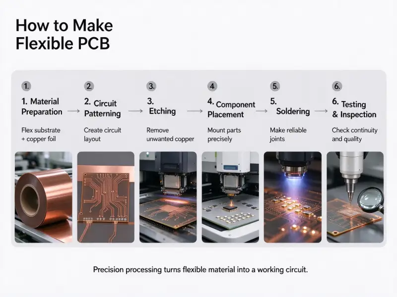
Rigid-flex PCB manufacturing follows the same imaging, etching, and plating steps as rigid boards but adds bonded flex layers and a three-dimensional assembly that needs closer handling and inspection.
Building the part is a layered process, and the flex regions demand cleaner registration than a flat board because any slip shows up as a misaligned transition.
Fabrication steps
The flow starts with imaging and etching the copper on both rigid and flex bases. The layers are then stacked and laminated with adhesive films under heat and pressure. Drilling and electroplating form the through-connections, and a coverlay is applied to the flex areas to shield the fine conductors. Automated optical inspection checks the flex features before assembly, since rework on a buried layer is difficult once the board is closed.
Assembly and testing
Components mount on the rigid zones, often with the board held in a fixture shaped to its final fold so placement stays accurate. Because the part is three-dimensional, test and inspection use specialized jigs and, at times, flying-probe or boundary-scan methods that suit odd geometries, rather than the flat-bed fixtures used for ordinary boards.
Advantages of rigid-flex PCBs
Rigid-flex PCBs save space and weight and cut the connectors and solder joints that most often fail, which raises reliability while often lowering total assembly cost.
The flexible tails remove separate cables, so the finished product gets smaller and lighter. Fewer connectors mean fewer cold joints and fewer points that vibrate loose over the product life. In many programs the higher board cost is offset by simpler assembly and fewer bought-in interconnect parts, and the single bonded path removes a class of wiring errors that plague hand-built harnesses.
Challenges and downsides
Rigid-flex PCBs cost more to design and build than plain rigid boards, and the flex sections add real downsides in signal integrity, thermal control, and testing.
The design rules are stricter, since bend radius, material mismatch, and layer transition all interact. Signal integrity and electromagnetic interference are harder to control across a moving substrate, and heat is tougher to sink through a thin flex zone that cannot carry a heavy ground plane. Testing a three-dimensional part needs special equipment, and a wrong material pair can fail under thermal cycling. Flexible PCBs on their own also show the same weak points: they are delicate to handle and poor hosts for heavy or high-pin components, which is exactly why rigid-flex keeps the components on the stable islands.
Flex PCB vs. rigid-flex PCB: what’s the difference
A flex PCB is fully flexible along its length, while a rigid-flex PCB keeps rigid areas for components and uses flex only where the path must bend, so the two differ in structure, cost, and where they fit.
The two are easy to confuse because both use polyimide and etched copper, but they are built for different jobs and fail in different ways.
| Aspect | Flex PCB | Rigid-flex PCB |
|---|---|---|
| Structure | All flexible | Rigid islands plus flex tails |
| Components | Few, on flex or bonded stiffener | Mounted on rigid sections |
| Bending | Continual where designed | Only in flex zones |
| Cost | Lower for simple links | Higher, fewer interconnect parts |
| Reliability | Good for light links | Higher for full assemblies |
Where rigid-flex PCBs are used
Rigid-flex PCBs fit products where space, weight, and reliability matter more than the higher board cost, which puts them in consumer, medical, automotive, and aerospace gear.
The board earns its price when a cable harness fails or will not fit inside the enclosure.
Consumer and medical
Phones, cameras, and wearables use rigid-flex to fold displays and sensors into thin bodies. In medical devices such as implantable monitors, the weight and reliability gain can outweigh almost any cost, because a failed interconnect inside a patient is not an option.
Automotive and aerospace
Advanced driver-assist and avionics systems pack computing into awkward spaces where a rigid-flex part replaces several boards and their connectors. The fewer joints survive vibration and temperature swings better than cabled links, and the saved mass helps in vehicles where every gram is counted. Industrial testers and instruments with moving arms use the same approach, where a flex tail must survive constant motion.
Rigid-flex PCB cost factors
Rigid-flex PCB cost is driven by material choice, layer and flex-branch count, build yield, and volume, and many programs recover the premium through fewer bought-in parts and simpler assembly.
There is no single price per board because the variables move with the design. High-performance laminates and rolled copper cost more than baseline FR-4 and electrolytic copper. More flex branches and tighter layer counts lower yield and raise scrap, so a complex stackup costs more than a simple one even at the same footprint. At higher volumes, the saved connectors and assembly steps often pull the total installed cost back in line with a cabled rigid solution, which is why the board-to-board comparison alone can mislead.
How to choose a rigid-flex PCB manufacturer
Choose a rigid-flex PCB manufacturer that runs both rigid and flex processes in one line, follows IPC design standards, and supports design-for-manufacture before you release the file.
The risk in rigid-flex is the rigid-to-flex joint, so a shop that only plates flex or only builds rigid will struggle at the seam where the two meet. Ask whether the supplier works to IPC-2223 for the flex portions and offers DFM feedback on bend radius and stackup before fabrication. Consistent prototyping-to-production quality matters more than a low bare-board quote, because re-spins on a three-dimensional part are expensive and slow, and a supplier that has run similar folds can flag trouble while the design is still cheap to change.

FAQ
How long does a rigid-flex PCB last under repeated bending?
Life depends on the bend type and radius. Static flex-to-install folds see few cycles, while dynamic hinges are rated for hundreds of thousands to millions of bends when the radius follows the IPC-2223 ratio for the layer count. Prototype flex testing confirms the actual count for a given build, since copper grade and bend geometry move the number by a wide margin.
Can high-speed signals route through the flex section?
They can, but the moving substrate makes impedance control harder. Keeping trace width and dielectric constant steady through the flex zone, routing pairs as a tight twist, and avoiding ground-plane cuts at the bend help. For very high speeds, designers often keep the critical lanes on the rigid sections and use the flex only for lower-rate links, which protects signal quality without giving up the space-saving.
Do rigid-flex PCBs need special assembly equipment?
Not a separate line, but fixtures shaped to the folded form and inspection tuned to three-dimensional geometry are common. Standard pick-and-place handles the rigid zones; the difference is in holding the part steady during placement and in using test jigs that reach the odd corners a flat board would not have. The added tooling is modest next to the interconnect it removes.