A circuit board pattern decides whether a design can be built at all. It fixes where current flows, how wide the traces are, how many layers the board needs, and what the panel costs. When a PCB order stalls, the reason is usually the same: the pattern asks for geometry the factory cannot hold.
A circuit board pattern is the arrangement of copper traces, pads, vias, and planes that connects every component on a printed circuit board (PCB). It is design data, not hardware. Before ordering, check four things: trace width and spacing against the manufacturer’s stated minimums, layer count and stack-up, impedance and tolerance notes, and whether the data package is complete enough to quote.
The sections below follow the order in which a fabrication quote is built.

What a circuit board pattern is
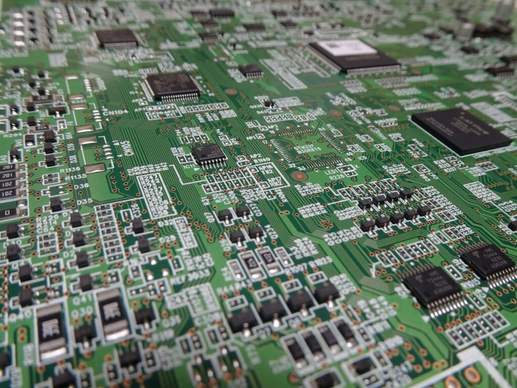
A circuit board pattern is the conductive geometry of a PCB: the traces that carry signals and power, the pads components solder to, the vias that link one layer to another, and the planes that distribute power and ground. Designers also call it the artwork or the layout data. It describes connections, not the physical board.
The pattern comes out of printed circuit board design. A designer draws a schematic, assigns a footprint to every component, places the parts, then routes copper between them. Export those copper layers one by one, and you have the pattern. Fabrication adds everything that is not copper: substrate, copper foil, solder mask, silkscreen, and surface finish. You are ordering files that a factory turns into tooling, drill programs, and imaging films, and any ambiguity in them gets filled with a guess.
Pattern, artwork, layout, and footprint
These four terms get used loosely, which causes problems in a request for a quote.
| Term | What it covers | Scope |
|---|---|---|
| Circuit board pattern, or artwork | Copper geometry layer by layer, plus drill and mask layers | The whole board |
| Layout | Placing components and routing the pattern | The whole board |
| Footprint, or land pattern | Pad geometry for one component package | A single component |
| Schematic | Logical connections drawn as symbols | No physical geometry |
A pattern can be right while a footprint inside it is wrong. A chip resistor on the land pattern for the next size up still routes cleanly, but it will not solder, and the fault shows up at assembly.
What the pattern decides on the finished board
The pattern sets the electrical and thermal behavior of the board before a component is placed. Trace width and copper weight fix how much current a path carries, layer order and plane placement fix the return path, and spacing and routing topology fix what the board radiates and what noise it picks up.
| Pattern decision | What it settles | How it shows up when wrong |
|---|---|---|
| Trace width and copper weight | Current capacity and voltage drop | Warm traces, rails that sag under load |
| Trace length matching | Timing between related signals | Data errors on high-speed interfaces |
| Reference plane continuity | Return the current path and impedance. | Radiated emissions, ringing |
| Via count and placement | Layer transitions and heat paths | Hot spots under power packages |
Impedance and signal integrity
Trace width, dielectric thickness, and distance to the nearest reference plane set the characteristic impedance of a trace. An impedance note tells the factory which value to hold and on which layers. Leave it out, and impedance lands wherever the etch process puts it.
Power delivery and return current
Copper weight matters as much as width. A 1 oz layer holds 35 µm of copper; a 2 oz layer holds 70 µm. Doubling copper roughly halves the width needed for the same current at the same temperature rise. The IPC-2221 current-carrying formula ties capacity to cross-sectional area and the temperature rise you allow. Outer traces shed heat into air; inner traces sit inside insulating laminate, so the same current needs roughly twice the width.
EMI, shielding, and heat
Emissions track loop area. A signal whose return path runs far from the trace forms a loop, and that loop is an antenna. Routing the return directly under the signal closes it and drops the emission. Heat follows a different rule: it needs copper and a path to a plane, which is what thermal vias under a power package provide.
The main pattern types and where they fit
Pattern type is a layer-count decision before it is anything else. Single-sided and double-sided patterns cover simple and moderate circuits at the lowest cost. Multilayer patterns add inner signal and plane layers for density and controlled impedance. Power plane, ground plane, differential pair, clock distribution, and RF transmission line patterns sit inside those layer counts rather than standing alone.
| Pattern type | Layer structure | Fits | Demands from the factory |
|---|---|---|---|
| Single-sided | One copper layer | Simple, low-density circuits | Basic etch and drill |
| Double-sided | Copper on both faces, linked by vias | Most control and interface boards | Plated through-hole process |
| Multilayer | Inner layers laminated between outer ones | Dense digital and mixed-signal boards | Layer registration, controlled lamination |
| Power and ground plane | Dedicated layers or large pour areas | Boards with several supply rails | Etch uniformity on copper areas |
| Differential pair | Paired traces at a set spacing | High-speed serial interfaces | Controlled impedance, tight etch tolerance |
| Clock distribution | Matched, tree, or grid-routed nets | Boards with synchronized devices | Length matching and skew control |
| RF transmission line | Grounded coplanar or microstrip geometry | Wireless and radar front ends | Impedance control, laminate consistency |
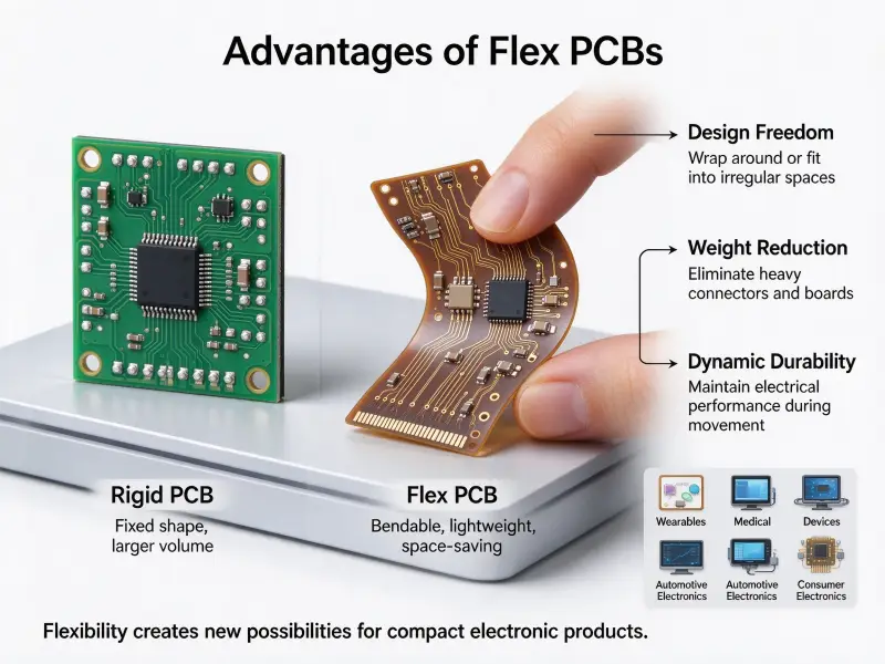
| Flexible and rigid-flex | Bendable laminates, sometimes with rigid sections | Devices that fold or flex in service | Specialized handling and bonding steps |
Two notes sit behind that table. Layer count drives registration difficulty, and registration drives yield, which is why a 4-layer and a 16-layer board sit on different price curves. Printed circuit board material matters too: a pair that holds impedance on one laminate may not on another.
Pattern dimensions and material that drive price, yield, and lead time
Price is set by how hard the pattern is to etch, drill, register, and laminate. Trace width and spacing set the etch class. Hole size against board thickness sets the plating aspect ratio. Copper weight sets etch time and panel uniformity. The laminate sets the dielectric stability your impedance depends on.
| Parameter | Why it matters | What it pushes up |
|---|---|---|
| Minimum trace width and spacing | Sets the etch class and imaging tolerance | Price and minimum order quantity |
| Minimum mechanical hole size | Sets drill bit life and registration margin | Breakage and requote risk |
| Annular ring | Sets the margin between drill and pad | Plating reliability, scrap rate |
| Board thickness against hole size | Sets the plating aspect ratio | Process control and price |
| Impedance tolerance | Sets whether coupons must be tested | Fixture and test cost |
Compare the pattern against the published capability sheet of the factory before you send it, not after. A design at the edge of a stated minimum gets requoted once it reaches engineering. Where you need tight numbers for voltage clearance or current capacity, work from the current revision of the IPC-2221B generic standard on the printed board design rather than a number you remember.
Laminate choice and printed circuit board material
The substrate constrains the pattern as much as the pattern constrains the substrate. A standard FR-4 build handles most digital and control work at the lowest cost. Raise the glass transition temperature, and the board survives more thermal cycles and heavier assembly heat. Move to a low-loss laminate, and the dielectric constant and dissipation factor become stable enough to hold a controlled-impedance RF pattern across the panel. The trade runs both ways, since a low-loss laminate costs more and etches differently.
What actually costs money?
Ordered by how much each item usually moves a quote:
- Layer count, which multiplies etch, lamination, and registration steps
- Minimum trace width and spacing below the standard class
- Copper weight above the standard foil
- Mechanical hole size below the standard drill range
- Impedance control with coupon testing
Absolute figures depend on the factory, the quantity, the panel utilization, and the delivery window, so quote the pattern you have rather than a general rule.
How the pattern connects to printed circuit board assembly
The pattern is the interface between fabrication and assembly. The paste mask decides how much solder lands on each pad. Thermal relief decides whether plane-connected pads can be soldered at all. Silkscreen clearance decides whether inspection software flags a board that is actually fine.
| Pattern feature | Effect on assembly | Defect when it is off |
|---|---|---|
| Paste the mask aperture against the pad size. | Controls solder volume per joint | Bridging or starved joints |
| Thermal relief on plane-connected pads | Controls heat loss during soldering | Cold joints, incomplete fill |
| Silkscreen clearance to pads | Keeps ink off solderable surfaces | Poor wetting, false inspection calls |
| Fiducials in the panel | Gives placement machines a datum | Shifted placement on fine-pitch parts |
| Pad symmetry on two-terminal parts | Balances solder force during reflow | One end lifting off the pad |
Fabrication and assembly are separate capability sets. A printed circuit board manufacturer’s list often mixes the two, so check which side of the line each supplier covers. A fabricator publishing tight etch limits may have no placement line, and an assembly house may buy boards elsewhere. Send both teams the same pattern revision, and confirm the assembly and fabrication drawings agree.
How to read a circuit board pattern without a schematic
Work from the outside in. Read the printed labels, find where power enters, group components into functional blocks, and then follow copper between them. You will not recover the netlist, but you will recover enough intent to judge whether a pattern is sensible.
- Read the silkscreen. Reference designators and part values give you the map legend.
- Find the power entry point. Trace from the input connector to the first regulators and their bulk capacitors.
- Identify the ground structure. Large unbroken copper areas are returns, and everything else references them.
- Divide the board into blocks. Power, control, input, output, and communication parts usually sit in separate clusters.
- Follow the copper. Wide traces carry power and thin ones carry signals.
- Check against the component datasheets. Typical application circuits show what the surrounding pattern should look like.
Two limits apply. Inner layers are invisible from the surface, so a multilayer PCB only reveals its full pattern through fabrication data or X-ray imaging. And reading a pattern tells you what it connects, not whether that was intended, so verify with a continuity check before you power anything up.
What to send in a pattern data package
Send enough data for the factory to build and quote without interpreting anything. At minimum: the copper, drill, mask, and silkscreen layers in a standard fabrication format; a stack-up drawing; an impedance table if you need controlled impedance; the performance class for testing; and the panelization requirements. Anything missing becomes an assumption, and assumptions get quoted and built.
| File or document | What it carries | What breaks without it? |
|---|---|---|
| Fabrication data, layer by layer | Copper, drill, mask, silkscreen geometry | The board cannot be built as designed. |
| Stack-up drawing | Layer order, dielectric thicknesses, copper weights | Impedance and thickness drift |
| Impedance table | Target values, tolerance, coupon needs | Controlled impedance goes unverified. |
| Drill table | Finished hole sizes, plated and non-plated | Wrong hole sizes or tooling |
| Performance class and test requirements | Acceptance criteria for the finished board | Disputes at goods-in |
| Panelization and process edge requirements | Panel size, rails, fiducials, break-away method | Handling damage, misalignment at placement |
One item belongs in the process rather than the package. Ask for a manufacturability review before the order is released. It costs nothing at that stage, and it is the last point where a pattern problem is cheap to fix.

FAQ
How do I check whether a pattern is too dense for standard fabrication?
Compare the smallest trace width, the smallest spacing, and the smallest mechanical hole against the fabrication class you are paying for. If any of the three sits below the standard class, the design has moved into a tighter process that affects price and lead time.
Does solder mask color affect the circuit board pattern?
Not the copper geometry, but it can affect how well the pattern is produced and inspected. Color changes imaging and inspection contrast on fine features, and some finishes are harder to hold at very small mask dams.
Can a pattern be changed after the boards are fabricated?
The board can be modified, but the pattern cannot be rewritten. Common field fixes are cutting a trace and adding a wire link or reworking a pad to accept a different part. Both consume space and create a revision someone has to track. More than a cosmetic change means a new pattern revision and a new build.