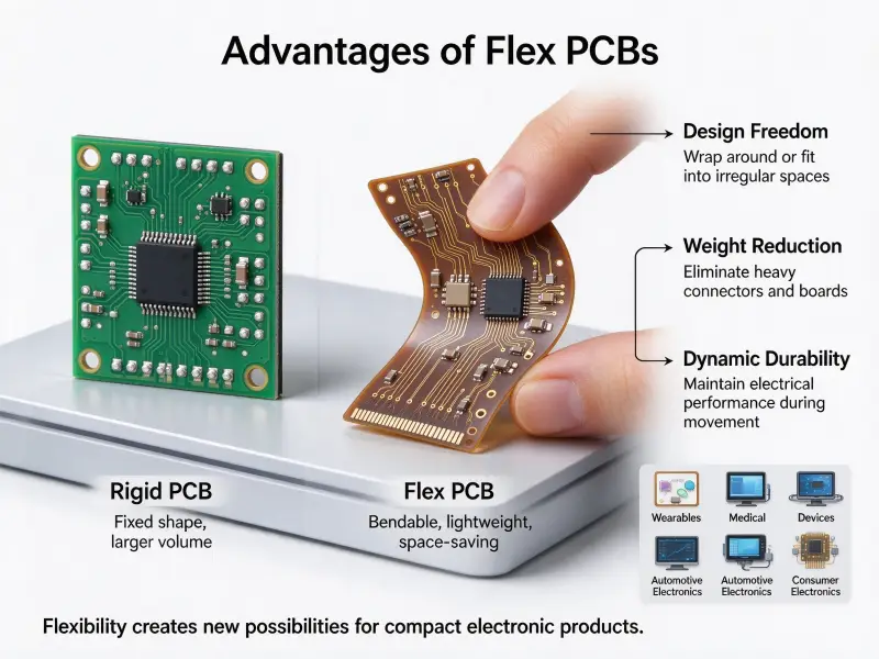
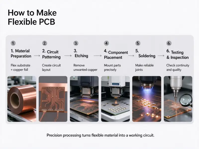
Open almost any electronic device, and the first thing you see inside is a flat board covered in copper lines under a colored coating. Most people describe it as a plastic sheet with metal tracks on it. That description is close enough to be useful and loose enough to cause real mistakes, because the material grade behind that flat sheet decides how much heat the board survives, how cleanly signals travel across it, and whether the finished assembly passes electrical tests on the first run.
A circuit board is built from an insulating substrate, normally woven glass fiber held in epoxy resin and known as FR-4, with copper foil bonded to it and etched into traces, pads, and planes. Partly cured resin sheets called prepreg glue the layers together, a solder mask covers everything except the pads, and a printed silkscreen carries the component labels. Flexible boards replace the glass-epoxy with polyimide film, radio frequency designs use PTFE or ceramic-filled laminates, and boards that run hot use an aluminum or copper base. Any panel produced by a custom PCB manufacturing line follows the same logic, because no single material does all four jobs at once.
The materials only make sense one at a time, so that is how this guide works through them.
What a circuit board is made of, layer by layer
A rigid board has four working layers: a substrate, copper conductors, a solder mask, and a silkscreen. Multilayer boards add prepreg and extra copper layers inside that stack.
Strip away the components, and what is left is a set of thin sheets bonded under heat and pressure. Each sheet has one job, and the values below are the ones you will find on a standard 1.6 mm rigid board.
| Layer | What it is made of | What it does | Typical value |
|---|---|---|---|
| Substrate | Woven E-glass cloth in epoxy resin, usually FR-4 | Holds everything rigid and insulates conductors from each other | 1.6 mm total board thickness |
| Copper | Electrodeposited or rolled foil, laminated, then etched | Carries signals, power, and ground | 1 oz equals about 35 µm. |
| Prepreg | Glass cloth pre-impregnated with partly cured resin | Bonds copper layers together during lamination | 0.1 to 0.2 mm per sheet |
| Solder mask | Photoimageable epoxy resin with pigment | Keeps solder off areas that should stay separate | 0.010 to 0.025 mm |
| Silkscreen | Non-conductive epoxy ink | Reference designators, polarity marks, board identification | About 0.010 mm |
Two of those layers cause most of the confusion. The substrate gets described as plastic, which is fair in the sense that epoxy is a polymer, but it is a thermoset. It cannot be melted and reshaped the way a thermoplastic bottle can, which is why board material is not recycled by remelting it.
Copper is the other one. The foil starts as a continuous sheet laminated across the whole panel, and the fabricator etches away everything the design does not need. Nothing is printed in conductive ink on a standard board. The word printed describes the imaging step that defines the pattern, not an inkjet process.
How copper weight relates to current
| Copper weight | Nominal thickness | Where it usually ends up |
|---|---|---|
| 0.5 oz | About 17 µm | Fine-pitch signal layers on dense boards |
| 1 oz | About 35 µm | The default for general-purpose boards |
| 2 oz | About 70 µm | Power supplies and motor control |
| 3 oz | About 105 µm | High-current industrial designs |
| 4 oz and above | 140 µm and up | Heavy copper, busbars, high-power conversion |
Copper weight is quoted in ounces per square foot of foil, and the conversion to micrometers is fixed at roughly 35 µm per ounce. Heavier copper carries more current and spreads heat better, but it also limits how fine traces and gaps can be, because etching thick foil evenly is harder. There is no single amp rating for a given trace. Current capacity comes from trace width, copper weight, the layer the trace sits on, and the temperature rise the design allows, which is why fabricators work from standard charts rather than one number.
Foil types and where each one is used
Electrodeposited copper is grown onto a rotating drum and has a columnar grain structure. Rolled and annealed copper is reduced mechanically, which leaves a more uniform grain that bends without cracking. Rigid boards almost always use electrodeposited foil. Flexible circuits tend to use rolled and annealed copper, because a flex circuit folded during installation puts repeated strain on its conductors.
What material is used for circuit boards?
FR-4 covers the large majority of boards made today. The alternatives are variations on the same idea: an insulator, a conductor, and a resin that holds the two together.
FR-4 dominates because of consistency rather than peak performance. Laminate grades have to repeat batch after batch, since a board shop cannot retune its whole process for every order. The same reasoning explains why the cheaper paper-based laminates still exist for simple single-sided work.
| Base material | What it is made of | Property that matters | Where it gets used |
|---|---|---|---|
| FR-1 and FR-2 | Paper core with phenolic resin | Low cost, punchable, limited heat resistance | Simple single-sided consumer boards |
| CEM-1 | Paper core with epoxy resin and one glass face | Better than paper grades, still single-sided | Low-cost appliances |
| CEM-3 | Non-woven glass core with epoxy resin | Close to FR-4 at lower cost | Double-sided consumer boards |
| FR-4, standard grade | Woven E-glass cloth in epoxy resin, Tg near 130 to 140°C | Balanced cost, strength, and insulation | Most industrial and consumer electronics |
| FR-4, high Tg | Same construction with modified resin, Tg 170°C and above | Survives repeated lead-free soldering and thermal cycling | Automotive, power supplies, servers |
| Polyimide | Polyimide film or glass cloth in polyimide resin | Flexible, continuous service near 260°C | Flex and rigid-flex, aerospace, medical |
| PTFE | Polytetrafluoroethylene with glass or ceramic filler | Dielectric constant near 2.2 and very low loss | Radar, microwave, high-speed radio frequency |
| Metal core | Aluminum or copper plate plus a thermally conductive dielectric | Moves heat away from components | LED lighting, power conversion, motor drives |
| Ceramic | Alumina, or aluminum nitride | High thermal conductivity and stiffness | Power modules, high-brightness LEDs |
FR-4 and the laminates that sit next to it
FR-4 stands for flame retardant, grade 4, and the name comes from an older grading system that predates modern material standards. On a fabrication drawing, the laminate is normally called out against IPC-4101E, the specification for base materials for rigid and multilayer printed boards, which lets a designer name a material by specification sheet instead of by trade name. That matters when a second source has to be approved months into a program.
Halogen-free grades are a separate branch of the same family. They use a phosphorus-based flame retardant instead of brominated compounds, which changes the resin chemistry and usually the price, without changing the fact that the board still starts as glass cloth in resin.
When FR-4 is not enough
Polyimide earns its place in two situations: boards that bend and boards that live in heat. It absorbs more moisture than FR-4 and costs considerably more, so it rarely appears on a standard rigid build.
PTFE and ceramic-filled laminates exist for signal loss. At low frequencies FR-4 is fine, but its dielectric loss rises with frequency, and above a few gigahertz the losses turn into a real design constraint. PTFE has a much lower dielectric constant and loss tangent, at the price of being soft, dimensionally awkward, and difficult to drill, plate, and bond.
Ceramic substrates take the opposite trade. Alumina and aluminum nitride are stiff, stable, and conduct heat well, which suits power modules where the heat path matters more than the cost.
Metal-backed boards for heat
A metal core board swaps the glass-epoxy substrate for an aluminum or copper plate with a thin thermally conductive dielectric on top. The metal spreads heat sideways and into the chassis, which is why lighting and power boards use it. Most metal core designs are single-sided or simple double-sided, since building many layers on a metal base gets expensive quickly.
What are green circuit boards made of?
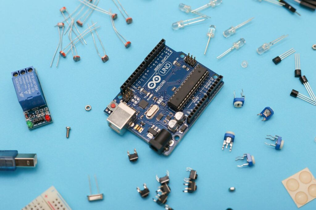
A green board is an ordinary board. The color comes from the solder mask coated over the outer copper, not from the substrate, and it has no effect on electrical performance.
What the green layer actually is
Solder mask is a photoimageable epoxy. It is applied as a liquid, exposed through a film, developed so that pads and vias stay open, and then thermally cured into a hard protective skin. In that sense it is a processed polymer coating, not a paint. Its three jobs are to stop solder bridging between adjacent pads, keep copper from oxidizing before assembly, and protect the surface from handling damage.
Green pigment is simply mixed into the resin. The same base chemistry is available in red, blue, black, white, and matte finishes.
Why green is the default, and whether the color matters
Green happens to be a good color for inspection. The contrast between the green surface, the exposed copper pads, and the white legend makes missing or misaligned features easier to catch under a microscope and on automated optical inspection, which matters more than it sounds when you are checking thousands of boards a day. Green resin chemistries also have decades of process history behind them, so they behave predictably.
Every other color is a branding or aesthetic choice. Black and dark blue make visual inspection harder because they reflect less light, but they solder and insulate the same way. If a supplier quotes a different price for a different mask color, that reflects setup and material availability, not a change in the board.
What are flexible circuit boards made of?
Flexible circuits replace the rigid glass-epoxy core with polyimide film, usually between about 12 µm and 50 µm thick, and replace electrodeposited copper with rolled and annealed copper.
Polyimide and the adhesive question
There are two constructions. Adhesive-based flex uses a polyimide film, a layer of acrylic or epoxy adhesive, and copper foil. Adhesiveless flex bonds copper directly to the polyimide, either by casting it onto the film or by laminating it without glue.
Adhesiveless stacks are thinner, bend more reliably, and hold up better at high temperature, so they dominate where the circuit has to flex repeatedly. Adhesive-based stacks still make sense for a single fold during assembly, where the lower material cost matters more than flex fatigue.
Copper, coverlays, and stiffeners
A flex circuit needs protection on both sides. A coverlay is a polyimide film with adhesive that is laminated over the finished traces, while a covercoat is a screen-printed or photoimageable coating. Coverlay costs more and performs better; covercoat is cheaper and adequate for static bends.
Stiffeners are local pieces of FR-4, polyimide, or aluminum bonded to the board where a connector, switch, or component pad needs rigidity. They are the reason a flex design can be thin and flexible in the middle and stiff at the ends.
Where a product needs rigid sections and flexible interconnects in one piece, both material systems end up in a single stack, which is how a rigid-flex PCB manufacturer supplier builds it by laminating polyimide flex cores between outer FR-4 layers.
What are computer circuit boards made of?
Computer circuit boards use the same material families at higher grades. The board inside a laptop, a server, or a graphics card is a multilayer FR-4 stack, often with high-Tg or low-loss laminate and eight to sixteen copper layers or more.
Higher-grade laminate
Two pressures push a computer board up the material ladder. The first is thermal: processors run hot and the board sees repeated cycles of heating and cooling, so a resin with a higher glass transition temperature keeps its dimensions and its drilled hole walls intact for longer. The second is signal integrity. Modern data rates make dielectric loss and dielectric constant stability real design parameters, so low-loss laminates appear wherever high-speed differential pairs are routed over any distance.
Denser routing
A computer board also carries far more copper structure than a simple control board. Inner layers are largely given over to power and ground planes, which lowers impedance and gives signals a clean return path. High-density interconnect builds add microvias and blind or buried vias so that routing can pass between layers without drilling through the whole panel. Pads on these boards are usually finished with electroless nickel immersion gold, because the surface has to stay flat enough for fine-pitch and ball grid array components.
None of that changes the material answer. It is still glass cloth, resin, and copper. What changes is the grade and the amount.
Are all circuit boards PCBs?
In everyday speech the two terms are interchangeable. In engineering they describe different things.
A PCB is the bare board: substrate, copper, mask, and legend, with no components fitted. A PCBA is that same board after the assembly step, when components are soldered on and the board has been tested. The distinction matters when you are quoting, because a bare board price and an assembled board price are built from different cost structures.
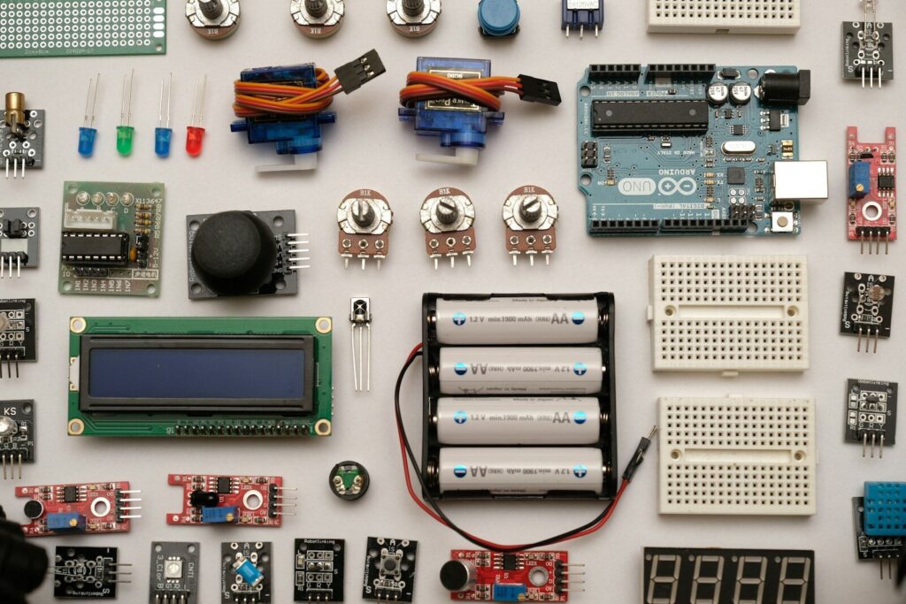
Some things people call circuit boards are not PCBs at all. A solderless breadboard is a block of plastic with spring clips. Stripboard and perfboard are pre-drilled insulator boards, not designed circuits made from copper foil. A ceramic substrate performs the same role as a PCB but is built from alumina or aluminum nitride rather than resin and glass. A wire harness connects boards together and is a separate product category entirely.
Are PCBs safe to touch?
Yes. An unplugged board is safe to handle. The materials are stable solids, and the real risks are mechanical and electrical rather than toxic.
What is actually on the surface
Bare copper oxidizes fast, so every exposed pad carries a surface finish. The finish is what your fingers actually contact.
| Finish | What sits on the pad | Why it gets chosen | Handling note |
|---|---|---|---|
| Lead-free hot air solder levelling | Tin-based solder, leveled with hot air | Low cost, easy to solder | Uneven surface, awkward at fine pitch |
| Electroless nickel immersion gold | Thin gold over a nickel barrier | Flat pads, long shelf life | Standard for dense and fine-pitch work |
| Immersion silver | Thin silver layer | Low loss at high frequency | Tarnishes, needs careful storage |
| Immersion tin | Thin tin layer | Flat and inexpensive | Tin whisker risk needs process control. |
| Organic solderability preservative | Organic coating over bare copper | Very flat, low cost | Short shelf life, handles poorly |
| Hard gold | Thick gold plating over nickel | Survives repeated plugging and rubbing | Used only on edge connectors and keypads |
None of these finishes is absorbed through skin. Gold, nickel, silver, and tin are bound in solid layers and do not rub off on your fingers during normal handling.
Handling practices that matter
Four things are worth doing. Disconnect power and let capacitors discharge before you touch anything. Follow anti-static practice, because a static discharge you cannot feel is still enough to damage a component. Watch the cut edges of a depanelized board, since glass fiber reinforced laminate leaves sharp edges and splinters. And wash your hands after handling old equipment, mainly because of dust and flux residue rather than the board material itself.
FAQ
Is it worth scrapping circuit boards?
Rarely, and almost never at home. Boards do contain recoverable copper along with small amounts of gold, silver, and palladium on plated areas, but the amount per board is small, and separating the metals is the hard part. Industrial recyclers make the economics work through volume and proper smelting equipment. Acid baths and open burning recover only part of the metal, are hazardous to the people doing them, and are not something to attempt. If you have accumulated old boards, a licensed e-waste collection point is the practical route and usually free.
Do circuit boards contain lead?
Modern boards generally do not. Restrictions on lead in electrical and electronic equipment came into force in the European Union in 2006, and most manufacturers moved to lead-free solder alloys and lead-free surface finishes such as lead-free hot air solder levelling and electroless nickel immersion gold. Older equipment, some exempt applications, and some specialist high-reliability assemblies still use tin-lead solder. In a finished board the lead is locked into the solder alloy, so handling is not a concern; the risk sits in soldering fumes and in waste processing.
How does the base material affect what a board costs?
The base material is one line in a quotation and usually not the largest one. The bigger drivers are layer count, board size, copper weight, surface finish, and dimensional tolerance. Laminate choice still moves the number in a predictable direction: standard FR-4 is the cheapest option that works for most designs, high-Tg and low-loss grades cost more before you add a single layer, and heavy copper costs more in both material and process time because thick foil etches more slowly and holds looser tolerances. The practical advice is to specify the grade the product actually needs, not the best grade available.