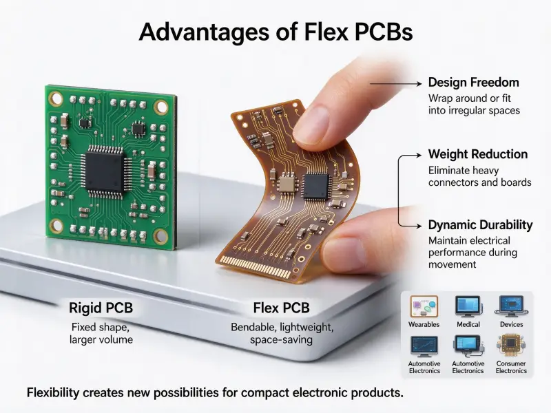
Every electronic device, from a kitchen thermostat to a ground-control rack, depends on one quiet component to carry power and signals where they need to go. That component is a populated board, and getting it right decides whether a product ships on time, passes certification, and stays reliable in the field. For engineers and procurement leads, the gap between a bare substrate and a finished board is where most cost, risk, and schedule risk actually live.
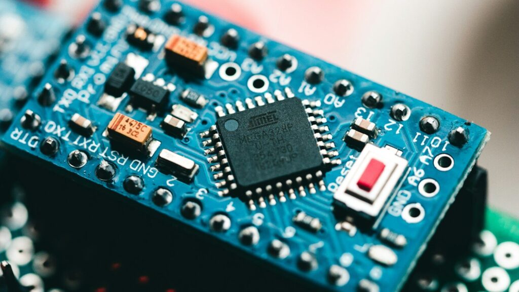
A circuit card assembly is a bare printed circuit board (PCB) with all its electronic parts soldered in place, tested, and ready to function as a complete subsystem. The terms “printed circuit board assembly” and “circuit card assembly” describe the same finished object: a board that can actually do work, not just a copper-etched blank. When you buy one, you are buying a process, not a single part.
If you are scoping a build, the fastest way to remove guesswork is to talk to a team that runs the whole flow under one roof, from bare board to box build, through PCB assembly services that cover fabrication, component sourcing, and test.
What a circuit card assembly actually is
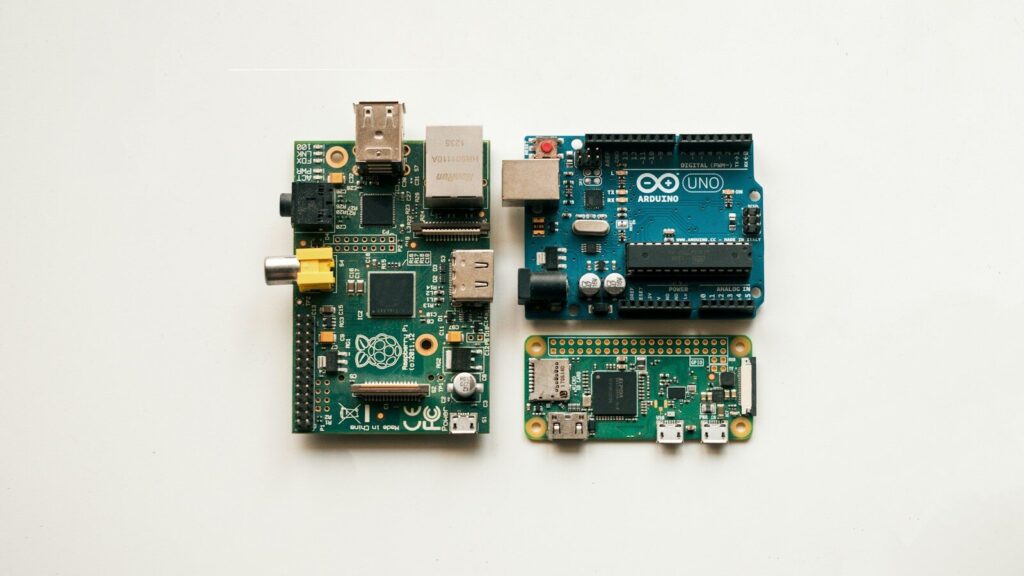
A circuit card assembly is the bonded result of a bare board and its components. The bare printed circuit board only carries the copper traces; the assembly is what happens after resistors, ICs, connectors, and passive parts are placed and soldered.
A bare board is little more than an insulated sheet with patterned copper. It cannot switch, amplify, or store anything on its own. The printed circuit board assembly step turns that sheet into a working circuit by fixing components to the pads and joining them to the traces. Once populated and inspected, the board becomes a circuit card assembly that can be dropped into a larger product.
The distinction matters for buying because the two halves of the job have different cost drivers. Board fabrication is about laminate, layer count, and trace geometry. Assembly is about placement precision, solder quality, and yield. A supplier that controls both, like a shop offering custom PCB manufacturing, can usually give a tighter total cost and a single point of accountability than one that only does one step.
Most teams use the terms interchangeably in conversation, and that is fine. What you should be precise about is scope: does your quote include the bare board, the parts, the stencil, the test, and the conformal coat, or only the labor to place parts you already own?
What a printed circuit board is made of
A circuit card assembly is only as solid as the bare board underneath it, and the bare board is mostly three things working together: a non-conductive substrate, a pattern of copper, and a thin coat of protection on top. Understanding those layers helps explain why two boards that look alike on a screen can behave very differently once powered.
Conductive copper layers and traces
Copper is the part of the board that actually does the work. It forms the traces, pads, and planes that carry current and signals between components, so it is fair to call copper the nervous system of the printed circuit board material.
A thin sheet of copper foil sits on top of the substrate, and in most boards that foil is etched into the familiar web of lines you see under the solder mask. Those lines are the traces, and they act as wires drawn directly into the board instead of running across it. Where a net needs to move real current rather than just a signal, the trace opens out into a pour or a plane, a broad area of copper that spreads heat and carries load without overheating.
Copper thickness is measured in ounces per square foot, written as copper weight. A 1 oz layer is roughly 35 micrometers thick. A 2 oz or 3 oz layer is specified where higher current has to flow, such as power stages and motor drives. Heavier copper costs more and is harder to etch cleanly, so it is called for only when the design truly needs it. Too little copper forces narrow traces that heat up and drop voltage under load, which is one of the quieter ways a board fails in the field.
Most boards are not single-layer, either. Inner layers stack the copper between sheets of substrate, and vias punch through to connect one layer to the next. More layers mean more routing room, but also more lamination steps and tighter registration, which is why layer count sits near the top of any fabrication quote.
Trace width and current capacity
A trace is only as good as its width relative to the current it carries. Size it too narrow for the amperage, and the trace heats up, sags in voltage, or fails outright. Designers reach for published charts and field solvers to set trace width, balancing the space available on the board against the current each net must handle.
This is one place where good printed circuit board design pays off. A board can be electrically correct on paper and still fail because its copper cannot deliver the current the circuit draws in real use. A 10 amp net routed on a 0.2 mm trace meant for a signal will cook long before the silicon complains. The fix is rarely exciting: widen the trace, move to a heavier copper weight, or split the current across parallel paths.
Temperature rise is the number designers watch. A wider trace stays cooler at the same current, and a cooler trace holds its resistance and its solder joints. On dense boards where space is tight, the compromise is real, and that is exactly where early review with the fabrication shop saves a respin.
The solder mask and silkscreen
Two thin layers sit on top of the copper, and both exist to keep the board buildable and serviceable. The solder mask protects the copper from oxidation and accidental shorts, while the silkscreen adds the text and symbols that make a board readable to the people who assemble and repair it.
The solder mask is the colored coating, usually green but increasingly black, blue, or red, that covers most of the copper. It leaves only the pads and exposed areas open so solder can form joints. Without it, stray solder could bridge two traces and create a short, and the copper would oxidize quickly in storage and use. A quality mask also sharpens the board’s appearance and makes automated optical inspection more reliable, because the camera has a clean background to read against.
The silkscreen is the layer of white, and sometimes yellow or black, printing on top of the mask. It carries component outlines, pin 1 markers, test-point labels, and the reference designators like R1 or U3 that let a technician find a part during assembly and repair. A clear silkscreen cuts assembly errors and speeds up debugging, which matters on dense boards where components sit millimeters apart and a missing label can turn a five-minute fix into an hour of tracing.
Together these layers decide more than looks. They set how much current the board can move, how well it survives handling, and how fast a line or a bench can work with it. Getting the substrate, copper, and coatings right is the unglamorous half of building a circuit card assembly that actually holds up.
How a circuit card assembly is built
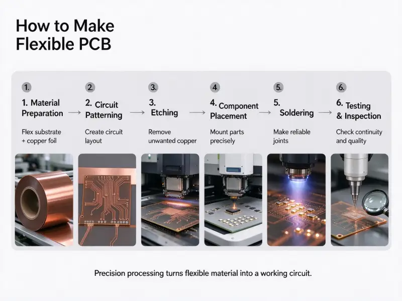
The build follows a repeatable sequence, and each step either protects yield or quietly destroys it. A competent circuit card assembly manufacturing process lines up solder paste, placement, reflow, and inspection so that defects are caught early, not after the board is boxed.
The core flow looks like this:
- Solder paste printing deposits a thin, shaped layer of paste onto the pads through a stainless stencil.
- Pick and place surface components onto the paste using high-speed, vision-guided heads.
- Reflow soldering melts the paste in a controlled thermal profile so joints form without cold or bridging defects.
- Through-hole insertion handles leads that pass through the board, either by wave solder or selective solder.
- Cleaning removes flux residue that could corrode contacts or disturb high-impedance signals.
- Inspection and test confirm placement, joints, and function before the board leaves the line.
The table below shows where the circuit card assembly process tends to lose yield and what a disciplined line does about it.
| Process stage | Common failure | Typical control |
|---|---|---|
| Stencil print | Insufficient or smeared paste | Automated paste inspection, stencil tension checks |
| Pick and place | Tombstoning, misalignment | Vision alignment, feeder audits |
| Reflow | Cold joints, voids | Profiled ovens, thermal coupons |
| Wave or selective | Skips, bridges | Solder pot maintenance, nozzle control |
| Final test | Latent function faults | ICT, flying probe, functional test |
Through-hole work still shows up on boards with connectors and high-power parts, so the circuit card assembly process is rarely pure surface-mount. Mixed technology is the norm, and the line has to handle both without slowing the surface-mount pass.
SLPCBA runs these steps as a linked sequence rather than disconnected stations, which keeps handling low and traceability high. When one team owns fabrication, placement, and testing, a bad joint is tied back to a specific profile and corrected before the next panel runs.
Designing for reliable circuit card assemblies
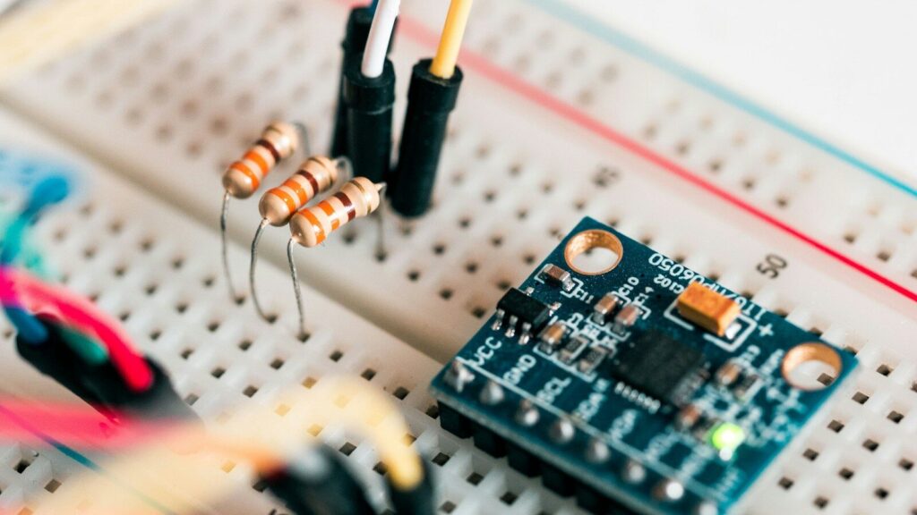
Good assemblies start on the design side, long before the first board is cut. Circuit card assembly design choices decide whether a board is cheap to build or a constant source of rework.
Layout and footprint discipline
Footprints must match the real parts, not the catalog guess. A pad that is a tenth of a millimeter off will place fine in the machine and then fail reflow at volume. Keeping printed circuit board design rules tight on pad size, clearance, and orientation removes most first-article surprises.
Design for manufacturing
DFM means designing so the line can build the board the first time. That covers panelization for the stencil, fiducials for the vision system, and keeping fine-pitch parts away from board edges where they are hard to inspect. A board built with DFM in mind needs fewer special fixtures and fewer operator decisions, which raises yield.
Material choices
The printed circuit board material sets how the board behaves under heat and load. Standard FR-4 covers most work, but RF, automotive, and power boards often need controlled-dielectric or metal-core laminates. Picking the material with the process in mind, not just the schematic, avoids warpage in reflow and drift in the field.
A design review before tooling pays for itself. Catching a footprint error at the schematic stage costs minutes; catching it after a thousand boards are built costs a recall. Teams that offer PCBA contract manufacturing usually fold this review into the handoff so the build starts clean.
Circuit card assemblies and modules
Breaking a product into assemblies and modules lets teams reuse proven blocks instead of re-deriving the same board for every variant. Circuit card assembly and modules is the practice of building self-contained subsections that snap into a larger system.
A module might be a power stage, a sensor front end, or a compute card. Building it as its own circuit card assembly means it can be tested alone, stocked alone, and swapped without tearing down the host product. For companies that ship several product versions from one platform, modular assemblies cut both inventory and risk.
The trade-off is interface discipline. A module is only useful if its connectors, firmware, and mechanical footprint stay fixed while everything around it changes. Spend the effort there, and the rest of the product line moves faster with fewer surprises.
How to choose a circuit card assembly manufacturer
Picking a builder is less about the lowest piece price and more about total risk across the program. Strong circuit card assembly manufacturers show their capability in certifications, test depth, and how they handle your parts.
The table below frames what to weigh when you compare shops.
| What to check | Why it matters | Red flag |
|---|---|---|
| Certifications (ISO 9001, IPC, RoHS) | Proof of a controlled process | No documented quality system |
| Component sourcing | Fake parts ruin a run. | Unverified open-market buys |
| Test coverage | Catches faults before ship | Visual only, no ICT or functional |
| Lead time and volume | Matches your ramp | Vague or shifting dates |
| Single-source vs. turnkey | One accountable owner | Finger-pointing between shops |
Experienced printed circuit board manufacturers will also show you their DFM feedback, their scrap rate, and how they handle obsolescence when a part goes end-of-life mid-program. Those answers tell you more than a price sheet.
Slpcba builds to IPC acceptability standards and keeps the supply chain inside one managed flow, so a procurement lead gets one quote, one schedule, and one responsible party instead of three vendors to reconcile.
Testing and quality standards that matter
Test is where a cheap board and a dependable board finally separate. The acceptance benchmark most shops build to is IPC-A-610, the workmanship standard published by IPC, which defines what a good joint looks like.
A real test plan stacks methods. Automated optical inspection catches placement and solder faults at speed. X-rays see underball-grid parts that optical cannot. In-circuit test checks each net against the schematic, and functional test confirms the board does its job in a simulated use case. RoHS compliance, governed by the EU directive tracked by the European Commission, keeps restricted substances out of the build for regulated markets.
Skipping tests to save a few cents per board move costs downstream to field returns, where it multiplies. The right test depth depends on volume and application: a toy needs less than a flight control board, but both deserve a defined plan rather than hope.
Cost drivers and how to keep them under control
Board cost is not one number; it is the sum of several levers, and most are set by design before a quote is ever requested. Understanding them lets you trim spend without trimming reliability.
The biggest drivers are layer count and board size, component count and package mix, test depth, and order volume. Fine-pitch and ball-grid parts need more careful placement and X-ray, which adds cost. Tight tolerances on impedance or material push fabrication cost up. Low volumes lose the economies of panelization and setup amortization.
You can pull cost down without hurting the product by relaxing specs that do not affect function, consolidating parts to fewer line items, and designing for standard laminates where the circuit allows. A builder offering electronic manufacturing solutions will usually walk through these trade-offs with you and show where each dollar goes, so you can decide what to keep and what to cut.
Volume remains the strongest lever. A board that is painful at fifty units often looks healthy at five thousand once setup and tooling spread across the run. Plan the ramp with the supplier early so the line is ready when demand arrives.
If you are ready to scope a build, the practical next step is to send the gerbers and bill of materials to a team that can quote fabrication, assembly, and test together, then review the DFM feedback before you commit to tooling.
Frequently asked questions
What is the difference between a PCB and a circuit card assembly?
A PCB is the bare, unpopulated board with copper traces but no parts. A circuit card assembly is that same board after components are placed and soldered, so it can actually perform a function. People sometimes use the terms loosely, but the assembly is the finished, working item.
How long does circuit card assembly usually take?
Lead time depends on volume, component availability, and test depth. A small prototype run with parts on hand can move in days, while a production order waiting on long-lead ICs may take several weeks. The surest way to shorten it is to release the bill of materials early so sourcing starts before fabrication.
What certifications should a circuit card assembly manufacturer have?
At minimum, look for ISO 9001 for a managed quality system and IPC-trained operators for workmanship. RoHS and REACH compliance matter for regulated markets, and UL or ISO 13485 may apply for medical or safety-critical work. Ask for the current certificates and how they audit their own line.