Standard FR-4 boards still carry most of the world’s electronics, and they do it cheaply. But a growing share of designs asks for things a conventional two- or four-layer board cannot deliver. Signal integrity above 10 GHz, power density that pushes a board past what the solder mask tolerates, or a form factor that has to fold into a wrist-worn enclosure. That gap is where advanced circuit boards live, and it is also where most sourcing mistakes get made, because the term means different things to different suppliers.
Advanced circuit boards are printed circuit boards built with structures, materials, and tolerances that go beyond conventional FR-4 fabrication. The category covers high-layer-count multilayers, high-density interconnect builds with laser-drilled microvias, high-frequency and high-speed laminates, rigid-flex constructions, heavy copper and metal-core boards, and ceramic substrates. What makes a board advanced is not one feature but the combination of finer geometry, controlled impedance, tighter layer registration, and certified acceptance criteria, usually IPC Class 2 or Class 3 rather than the baseline commercial specification.
This guide covers how the category is defined, what each board type actually solves, and what to verify before you hand a design to an HDI PCB manufacturer.
What counts as an advanced circuit board?
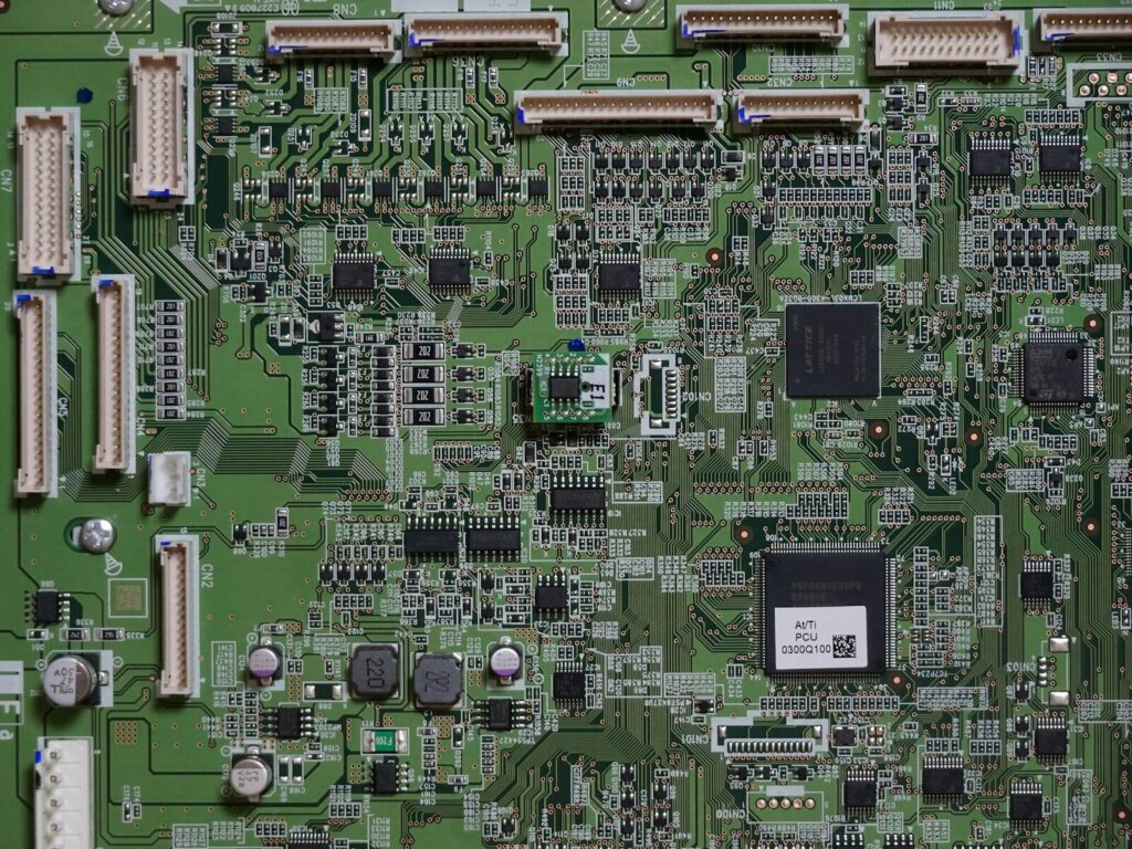
An advanced circuit board is one whose electrical, thermal, or dimensional requirements exceed what standard FR-4 double-sided or low-layer-count fabrication can reliably produce. The dividing line is measurable rather than promotional: layer count, minimum trace and space, minimum microvia diameter, copper weight, material loss behavior, and the IPC performance class written on the fabrication drawing.
Where the line sits between standard and advanced boards
The clearest way to classify a design is to compare it against the fabrication capabilities that ordinary shops can hold across a full production run. Any single parameter below can be pushed further in a prototype, but holding it in volume is what separates an advanced build from a stretched standard one.
| Parameter | Standard board | Advanced board | Why it matters |
|---|---|---|---|
| Layer count | 1 to 8 | 8 to 40 and above | Dedicated power and ground planes, clean high-speed return paths |
| Trace width and spacing | 4 to 6 mil | 2.5 to 3 mil, finer for substrates | Escapes from 0.4 mm pitch and smaller ball grid arrays |
| Smallest via | Mechanically drilled, around 0.2 mm | Laser-drilled microvia, 0.075 to 0.15 mm | Routing density and shorter signal paths |
| Copper weight | 1 to 2 oz | 2 to 10 oz and above | Current carrying in power stages and busbars |
| Base material | Standard FR-4 | High-Tg FR-4, low-loss laminate, PTFE, polyimide, ceramic, metal core | Insertion loss at gigahertz frequencies, heat path |
| Impedance control | Often unspecified | Specified and verified, tight tolerance | Reflections, crosstalk, eye-opening |
| Acceptance class | Class 1 or 2 | Class 2 or 3, with test coupons | Field reliability in critical systems |
The capabilities that define an advanced build
A handful of process capabilities recur across every advanced board, regardless of the end market. High-density interconnect structures use blind, buried, and stacked microvias to move signals between layers without consuming surface area. Sequential lamination builds the stack in multiple press cycles, which is how HDI layer counts get beyond what a single press can handle. Back drilling removes the unused stub of a plated through hole, a defect that matters more as data rates climb because the stub behaves as a resonant antenna. Via-in-pad places the via directly under a component pad and fills it with conductive or non-conductive material before plating over.
Add to that thick copper for current, embedded cavities for components that sit inside the board, and a controlled-impedance discipline that ties every trace geometry back to a verified stack-up. Layer counts above 30 are routine in switch and backplane work, and the value of a single board rises sharply with each layer added because the yield risk compounds.
Types of advanced circuit boards and what each one solves
The advanced category splits into distinct board types, and each one exists to solve a specific constraint. HDI addresses density, high-frequency and high-speed laminates address signal loss, rigid-flex addresses geometry and connector count, and heavy copper, metal core, and ceramic boards address current and heat.
HDI and microvia boards
HDI boards use microvias, fine lines, and sequential lamination to pack more interconnect into less area. The practical trigger is component pitch. Once a design uses 0.4 mm pitch or finer, a conventional through-hole fanout runs out of room, and you either add layers or move to microvia structures. HDI also shortens signal paths, which helps electrical performance as a side effect of the density. Smartphones, wearables, camera modules, and AI accelerator boards all sit in this group.
High-frequency and high-speed boards
These are two different problems that often get merged in conversation. High-frequency work is about dielectric behavior at a specific band, where the dielectric constant and loss tangent of the laminate decide how much signal survives the trace. High-speed digital work is about rise time, impedance continuity, and the noise budget across a link.
The material choice separates them from standard builds. A high-frequency PCB usually runs on a PTFE-based or low-loss laminate with stable electrical properties across temperature, while a high-speed digital board can often stay on a low-loss FR-4 grade if trace lengths are kept in check. Frequency, not the marketing label, decides which you need.
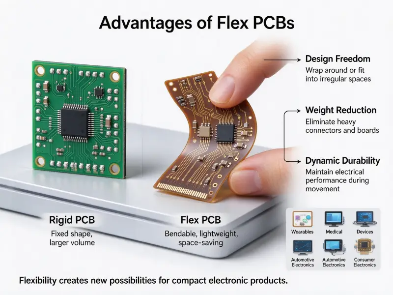
Rigid-flex and flex boards
Rigid-flex combines rigid sections for component mounting with flexible polyimide sections that bend. The payoff is fewer connectors, fewer solder joints, and a smaller assembly. A cable that used to be a separate part becomes part of the board, which removes two connector interfaces and the failure modes that come with them. Medical devices, aerospace payloads, camera assemblies, and portable instruments use this construction when the enclosure leaves no room for a conventional harness.
Heavy copper, metal core, and ceramic boards
When the constraint is current or heat rather than density, the answer changes. Heavy copper boards carry higher current and spread heat through the copper itself. Metal core boards use an aluminum or copper base under the dielectric to pull heat out of high-power components. Ceramic substrates, typically alumina or aluminum nitride, handle both high thermal load and high isolation requirements, which is why power modules and high-brightness lighting lean on them.
Advanced circuit board materials and stack-up choices
Material choice sets the ceiling on what a board can do. Standard FR-4 runs out of usefulness well before 10 Gbps because its dielectric loss turns long trace runs into attenuators. Every advanced design starts by matching the laminate to the frequency band and the thermal load, then building the stack-up around that choice.
| Material family | Dielectric constant, typical | Loss behavior | Common use |
|---|---|---|---|
| Standard FR-4 | 4.2 to 4.6 | Loss rises with frequency. | General digital, low-speed control |
| High-Tg FR-4 | 4.0 to 4.5 | Moderate | Multilayer boards exposed to repeated reflow and heat |
| Low-loss high-speed laminate | 3.3 to 3.9 | Low, stable into the tens of gigahertz | Servers, switches, high-rate serial links |
| PTFE-based laminate | 2.2 to 3.0 | Very low | Radar, RF front ends, antenna feeds |
| Polyimide | 3.4 to 3.6 | Moderate, wide temperature range | Flex and rigid-flex, aerospace, high-temperature service |
| Ceramic (alumina, aluminum nitride) | 8 to 10 | Low loss, high thermal conductivity | Power modules, high-brightness lighting |
Those figures are typical ranges for the material families, not specifications for a specific grade. Every laminate datasheet states its own values, and those are the numbers a stack-up review should use.
Matching material to frequency and thermal load
Two questions drive the decision. First, how much signal loss can the link tolerate over its longest trace? That sets the acceptable loss tangent at the operating frequency. Second, how much heat has to leave the board, and by which path? A board that dissipates 2 W through copper planes has very different material needs from one dissipating 60 W through a metal substrate. Material cost tracks performance closely, so specifying low-loss laminate across all layers when only two carry high-speed signals is an expensive habit.
Mixed-dielectric and hybrid stack-ups
Hybrid stack-ups combine material families in one board, usually placing RF layers on PTFE and digital layers on low-loss FR-4. This controls cost while meeting electrical targets, but it introduces a coefficient of thermal expansion mismatch between the materials. The lamination schedule has to account for that, and the fabricator needs to be involved before the layer assignment is frozen. Changing material assignment after tooling starts is one of the most expensive revisions a program can make.
Advanced PCB design: what changes at high speed and high density
Advanced design work adds three disciplines to a conventional layout: signal integrity, power integrity, and a manufacturability review that runs before the design is released rather than after it fails.
Signal and power integrity
Signal integrity in this context means controlling the return path, not just the trace. Every signal that leaves a driver needs a continuous reference plane under it, and every layer transition needs adjacent ground vias to keep the return current close. Differential pairs need matched length and spacing. Through-hole stubs should be removed by back drilling on the fastest nets. On the power side, the goal is a low-impedance power distribution network with enough decoupling at the right frequencies, which is a layout problem as much as a component selection problem.
Thermal and mechanical design
Heat leaves a board through copper, and the design decides how well. Thermal vias under power devices, copper pours on the planes they connect to, and in some cases a copper coin pressed into the laminate all create lower-resistance paths than the base material offers. Mechanical design matters just as much: a symmetric stack-up with balanced copper distribution avoids the warpage that makes fine-pitch assembly unreliable.
Designing for manufacturability
Most advanced designs fail on the shop floor rather than in simulation, and the failures cluster around a few details. Trace width that cannot be etched repeatably. Via aspect ratios that exceed what plating can fill. Annular rings that leave no registration margin. Layer counts that force a press cycle more than the schedule allows. A design rule check against the fabricator’s published capability, run early, costs almost nothing. The same issue was found after tooling costs a respin.
How advanced circuit boards are manufactured
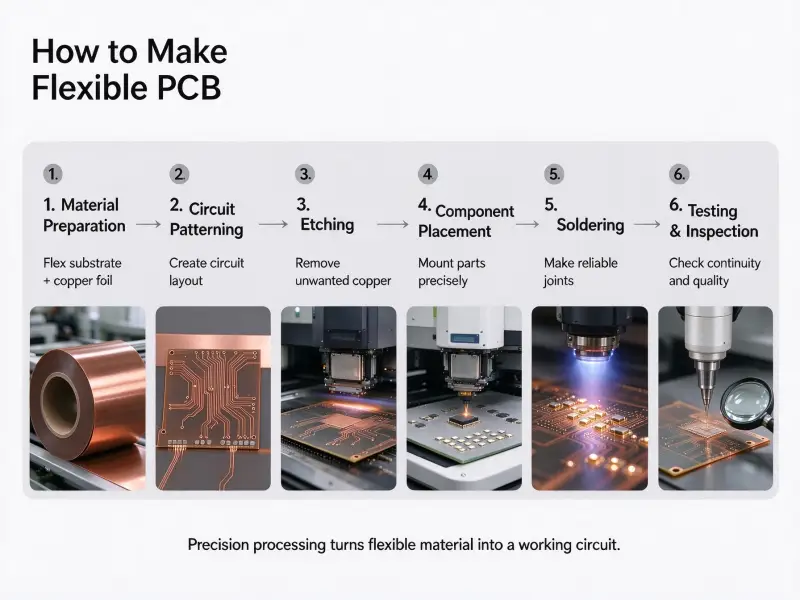
Advanced fabrication follows the same broad sequence as any multilayer board, but each step runs inside much tighter windows. Sequential lamination replaces single-press lamination, laser drilling replaces mechanical drilling for the smallest vias, and inspection is built into the process rather than bolted on at the end.
Process sequence
- Engineering review. Gerber data, stack-up, and design rules are checked against fabrication capability before anything is cut.
- Material preparation. Laminates are selected for frequency and thermal requirements, then stored under controlled humidity.
- Inner layer imaging. Laser direct imaging defines fine features with higher registration accuracy than film-based exposure.
- Lamination. Multiple layers bond under controlled heat and pressure; HDI builds on this step for each build-up cycle.
- Laser drilling. Microvias, blind vias, and buried vias are formed, followed by desmear and plasma treatment.
- Plating and via fill. Copper plating builds wall thickness to the acceptance class; via-in-pad structures are filled and capped.
- Outer layer imaging and etching. Fine-line features are defined and inspected.
- Surface finish. The choice among ENIG, immersion silver, immersion tin, hard gold, and OSP affects solderability and, at high frequency, insertion loss.
- Profiling and electrical test. Boards are routed to outline, then tested for continuity and isolation.
Inspection and test
Sequential process control matters more here because defects that a standard board tolerates become field failures at higher layer counts and tighter geometry.
| Method | What it catches |
|---|---|
| Automated optical inspection | Missing copper, nicks, and spacing violations after etch |
| X-ray inspection | Drill registration, inner layer alignment, via wall integrity |
| Impedance verification | Deviations between designed and as-built trace geometry |
| Microsection analysis | Plating thickness, hole wall quality, dielectric spacing |
| Thermal stress testing | Laminate separation and plating cracks after simulated assembly heat |
| 100% electrical test | Opens, shorts, and isolation failures across every net |
Quality standards and certifications buyers should look for
The standards to specify are IPC-6012 for rigid boards, IPC-6013 for flexible and rigid-flex, and IPC-6018 for high-frequency boards, each written alongside a performance class. The class, not the document number alone, is what sets the acceptance criteria your supplier has to hold.
Performance classes and acceptance criteria
Class 1 covers general consumer products where function is the only requirement. Class 2 covers dedicated service electronics that need a long, uninterrupted life, which includes most industrial, commercial, and automotive comfort systems. Class 3 covers high-reliability products where downtime is unacceptable: aerospace, defense, life-support medical equipment, and safety-critical automotive systems. The gap between Class 2 and Class 3 shows up in minimum hole wall plating, annular ring requirements, void limits in plated holes, and how often microsections and test coupons are pulled.
The current revision family is worth checking by name. IPC-6012F, released as the revision that expanded requirements for board cavities, copper wrap plating, back drilling acceptance, and microvia reliability, reflects industry experience with stacked microvias in high-layer-count HDI boards, which have been a known failure mode in the field. The IPC-6012F release notes from IPC spell out those changes; a specification that still cites an older revision is quietly applying a different acceptance standard.
Application-specific certifications
Beyond IPC, the relevant certifications depend on where the board ends up. Automotive programs usually require IATF 16949 and often AEC-Q qualification for the components. Medical devices require ISO 13485. Aerospace and defense programs expect AS9100, and some require ITAR-compliant handling of design data. Underwriters Laboratories recognition for the laminate and RoHS compliance for materials sit under all of these as baseline requirements. Certifications are not interchangeable, and a supplier that holds a general quality certificate but no automotive or medical system has not been audited for the process controls those markets need.
Industries that rely on advanced circuit boards
Advanced boards cluster in five end markets where failure carries a real cost: aerospace and defense, data centers and networking, automotive, medical devices, and industrial power and automation. Each one pushes a different constraint to the limit.
Aerospace, defense, and space
These programs optimize for reliability and environmental tolerance rather than cost or size. Boards are expected to survive thermal cycling across a range beyond what commercial hardware sees, often specified from around minus 55 to plus 125 degrees Celsius with thousands of cycles. Vibration, vacuum, and radiation exposure add requirements that affect material selection and, in some cases, construction: extended-length flex and rigid-flex assemblies have been used in deep-space instruments where mass and connector count have to be minimized.
Data centers, AI, and networking
This is where layer counts and board value are rising fastest. Accelerator modules and high-port-count switches need dense interconnect, low-loss material, and clean power delivery in the same board, and the industry’s own market data reflects it. Prismark estimates put the global HDI market at roughly $19.9 billion in 2026, up about 23 percent year on year, with AI server demand growing faster than the overall category (Prismark figures as cited in a 2026 interim report; checked 18 September 2026).
Automotive, industrial, and medical
Automotive electronics add a constraint the other markets do not have: volume. A design has to be manufacturable at high yield, not just buildable once. Radar modules, battery management, and domain controllers all use HDI, or high-frequency material. Industrial applications lean on heavy copper and metal core boards for motor drives and power conversion. Medical devices span the range from implantable and body-worn monitors, which need HDI and flex, to imaging systems that need high-layer-count multilayers with tight impedance control.
Advanced circuit board assembly and the PCB-to-PCBA handoff
The difference between a PCB and a PCBA is that assembly adds the components. An advanced board is not finished when fabrication ends, and the decisions made for fabrication constrain what the assembly line can do.
Why fabrication and assembly should share one stack-up owner
Fine-pitch components need flat boards. If the stack-up is not symmetric enough or the copper distribution is uneven, the board can warp during reflow and cause placement defects that have nothing to do with the placement equipment. Pad geometry, stencil aperture design, and via-in-pad treatment all have to be agreed upon between the fabricator and the assembler, which is why advanced programs benefit from routing both through one turnkey PCB assembly partner. When they sit with two unrelated suppliers, every stack-up change becomes a negotiation over where the defect originated.
How to evaluate an advanced circuit board supplier
Evaluate a supplier against your design’s hardest parameter, not its easiest one. Most capable shops can build a 12-layer board. What separates them is whether they can hold fine-line geometry, microvia aspect ratios, and impedance tolerance across a production run and document it.
Questions to ask before you send Gerbers
- What is the maximum layer count you build in production, and what is the current thick-to-thin aspect ratio you hold?
- What is your smallest production microvia diameter, and how is it drilled and filled?
- Which material families do you stock or source reliably, and what are current lead times on each?
- How do you verify controlled impedance, and what tolerance can you hold on a production panel?
- What inspection is standard versus optional, and what does a test coupon report include?
- Which performance class do you hold on your standard process, and what changes when a drawing calls for Class 3?
- What certifications cover the facility that will actually build the board?
- What is the escalation path when a manufacturability issue appears during engineering review?
What drives cost and lead time?
Cost in advanced fabrication tracks five things: material grade, layer count, number of lamination cycles, drilling method, and inspection burden. A low-loss laminate costs several times a standard FR-4 grade of the same thickness. Each sequential lamination cycle adds press capacity and yield risk. Laser drilling is slower than mechanical drilling and requires its own equipment. Class 3 acceptance pulls more test coupons and microsections out of the run. There is no standard multiplier that turns these into a price, because panel utilization and order quantity change the arithmetic. The right move is to tell the supplier which parameters are fixed by the design and which have room, then let them quote alternatives.
What a usable quote should include
A quote that only states a price per board cannot be checked. Ask for the stack-up drawing with material grades and thicknesses, the IPC document revision and performance class, the impedance tolerance and the nets it applies to, the surface finish, whether test coupons and a microsection report are included, and the lead time in production quantity rather than prototype quantity. It is also worth confirming whether electronic components sourcing sits inside the same scope, since a board quote that arrives without a component path leaves half the program unplanned. If any of those are missing, the comparison between two suppliers is not a comparison at all.
FAQ
Is an advanced PCB more expensive than a standard PCB?
Usually yes, and for reasons that are mostly structural rather than arbitrary. Advanced boards consume more expensive laminates, more lamination cycles, laser drilling time, and more inspection samples per lot. The useful comparison is cost per function rather than cost per board, because an HDI stack often reaches a target with fewer layers than a conventional through-hole design would need.
Can advanced processes be used for small prototype quantities?
Often, but not always economically. Microvias and sequential lamination carry fixed setup costs that spread poorly across ten boards, so prototype quantities may see an effective multiple of the volume price. The practical approach during development is to prototype on the process you intend to produce with, even at a higher unit cost, so that the electrical and thermal behavior you validate matches the board you will eventually buy.
Are high-frequency and high-speed boards the same thing?
No. “High-frequency” refers to work at a defined band where the dielectric properties of the material dominate performance, typically in RF and microwave circuits. “High-speed” refers to digital links where rise time and impedance continuity dominate, and those designs can often use a low-loss FR-4 grade. A board can be one, both, or neither, and the material and stack-up follow the answer.